Electron Ptychography:
Basics, Hardware, Algorithms & Applications

Prof. Dr. Philipp Pelz

FAU Erlangen-Nürnberg

https://pelzlab.science/public_presentations/#conference-talks

FAU Logo IMN Logo CENEM Logo ERC Logo Eclipse Logo

Outline — from diffraction patterns to quantitative imaging

Five threads: X-ray vs. electron ptychography, phase retrieval and direct methods, the 4D-STEM acquisition chain, iterative and 3D reconstruction, then fields in the same data.

Part 1 · X-ray vs. electron ptychography

Many ptychography concepts transfer from X-rays — but the physics and engineering diverge quickly. What changes when we swap photons for electrons?

1 · X-ray vs e⁻
2 · Phase & direct
3 · Acquisition
4 · Iterative & 3D
5 · Fields

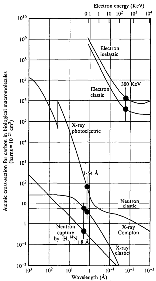
1. Strength of interaction — 1

Elastic scattering cross section for C of 300 keV electron is ~100.000× of 6 keV photon

Imaging single light atoms in 2D with electron ptychography is possible with some 10.000 e⁻/Ų

Chen, Z. et al. Mixed-state electron ptychography enables sub-angstrom resolution imaging with picometer precision at low dose. Nature Communications 11, 2994 (2020).


Imaging single light atoms in 3D with electron ptychography is possible with some 1M-10M e⁻/Ų

Cui, J. et al. Imaging, counting, and positioning single interstitial atoms in solids. Preprint at arXiv:2407.18063 (2024).

1. Strength of interaction — 2

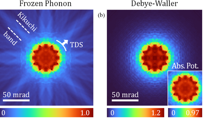
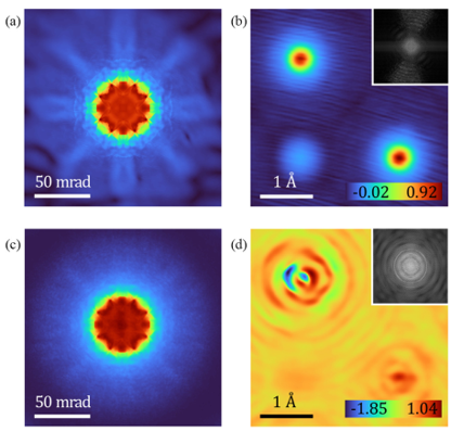
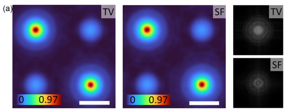
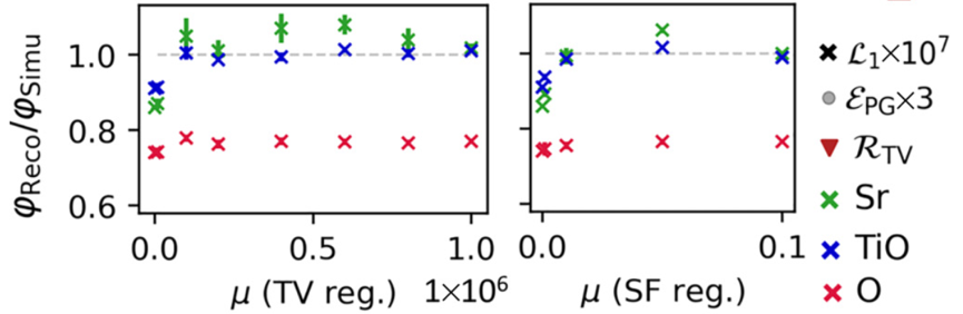
For algorithms: strong atomic potential peaks cannot be fully recovered by pixel-wise reconstruction

When dark-field data is measured, artifacts can arise using a pixelated model

Ideally, atomic peak height gives element

Quantification of recovered potentials is tricky, solution unclear yet

2. Depth of forward models

X-ray ptychography

\[ I_{j\mathbf{q}} = \sum_k \alpha_k \left| \langle \mathbf{q} | O_j | P_k \rangle \right|^2 \]

Electron ptychography

Coherent model

\[ I(\mathbf{s}) = \left| \mathcal{F} \left[ M(\phi(\cdot - \mathbf{s}), \mathcal{S}) \right] \right|^2 \]

\[ M(\phi, V_1, \dots, V_S) = e^{i\sigma V_S} \cdot \left(F \otimes \left(e^{i\sigma V_{S-1}} \dots \left(F \otimes \left(e^{i\sigma V_1} \cdot \phi\right)\right) \dots \right)\right) \]

\[ P(k, \Delta z, \theta) = e^{-i\pi\lambda k^2 \Delta z + 2\pi i \Delta z (k_x \tan \theta_x + k_y \tan \theta_y)} \]

Realistic model including atomic vibrations & spatial & temporal coherence

\[ V_{\mathrm{FP}}^{(j)}(\mathbf{r}, \tau) = \sum_{n=1}^{N} w_n v_{Z_n} \left( \mathbf{r} - \mathbf{r}_n - \sqrt{\langle u_n^2 \rangle} \cdot \mathbf{g}_{n,\tau} \right) \]

\[ I(\mathbf{s}) \approx \sum_k \alpha_k \left| \hat{M}_{\{\mathcal{S}\}}(\tau_k) \cdot \phi_{\{P\}}(\mathbf{r} - \mathbf{s} - \boldsymbol{\eta}_k, \delta_k) \right|^2 \]

Note

Atomic resolution allows direct parametrization
Voxels → Atoms

3. Degree of model mismatch

  • X-ray ptychography: weak interaction → thin-object / paraxial models usually match experiment
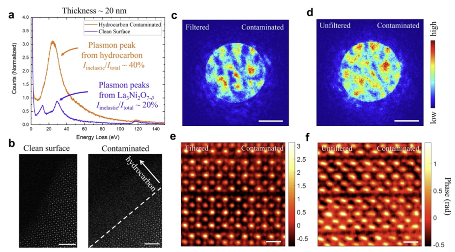
  • Electron ptychography: strong interaction → simplified models break down
    • inelastic/plasmon background and contamination
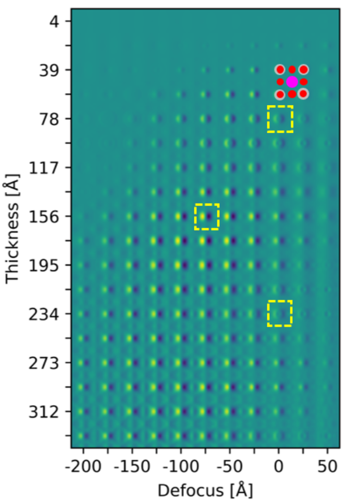
    • dynamical scattering vs. thickness and defocus

Adapted from Visualization of Oxygen Vacancies and Self-Doped Ligand Holes in La\(_3\)Ni\(_2\)O\(_{7-\delta}\) (n.d.): plasmons from hydrocarbon contamination on La\(_3\)Ni\(_2\)O\(_{7-\delta}\) — inelastic background in energy-filtered MEP.

Adapted from Deimetry et al. (2024): core-loss DPC images still contain elastic contrast — EFDPC at 10 eV beyond the Ti L\(_1\)-edge.

4. Experimental setup and resulting limitations

X-ray ptychography

  • Sample translation with piezos → few kHz max
  • FOV limited by sample translation

“2D images acquired at 110 kHz by combining the fast-acquisition scheme with a high-acquisition rate prototype detector” (Cipiccia et al. 2024)

“developed a new approach for scanning X-ray microscopy by combining a slow sample stage possessing a long travel range with a fast but small range positioner for the beam-defining optics” (Odstrçil et al. 2019)

Electron ptychography

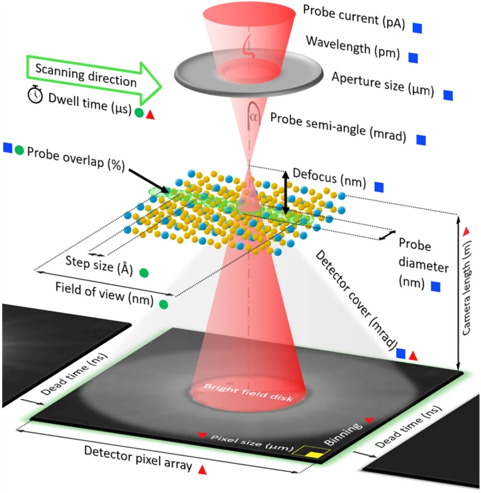
4D-STEM data acquisition

  • Beam translation with electron optics → few MHz max
  • FOV limited by electron optics → stitching scans

Note

Faster scans are coming to X-ray ptychography

4. Experimental setup and resulting limitations 2

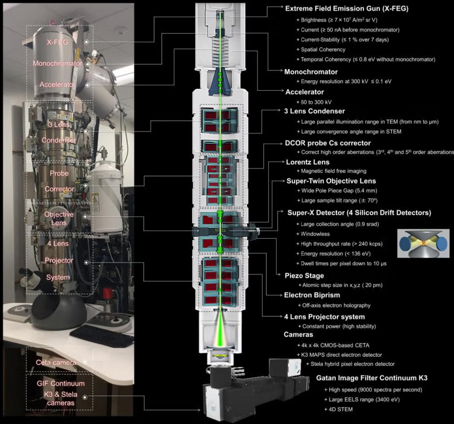
Optical elements and setup of a modern electron microscope

Part 2 · Phase problem & direct methods

Detectors record intensities; atomic structure lives in the phase. What can we retrieve directly — and when do we need iteration?

1 · X-ray vs e⁻
2 · Phase & direct
3 · Acquisition
4 · Iterative & 3D
5 · Fields

The Microscopy Phase Problem

  • The exit wave \(\psi(\vec{r})\) is complex; detectors record intensities \(I = |\psi|^2\)
  • Specimen structure is encoded primarily in the phase (weak objects: \(t(\vec{r}) \approx 1 + i\sigma V_p(\vec{r})\))
  • Conventional annular BF/ABF/ADF/HAADF signals integrate \(| \tilde{\psi}_\mathrm{exit}|^2\) and discard most phase information
  • 4D-STEM retains the full diffraction pattern \(I(\vec{R}, \vec{k})\) at every scan position — the raw material for phase retrieval

Note

TEM defocus and Zernike phase plates convert phase → intensity; STEM reciprocity links these ideas to convergent-beam 4D-STEM

From Scan Position to Diffraction Pattern

Note

Move the probe over the sample — structure is encoded in how the bright-field disk distorts. One pattern per scan pixel = 4D-STEM.

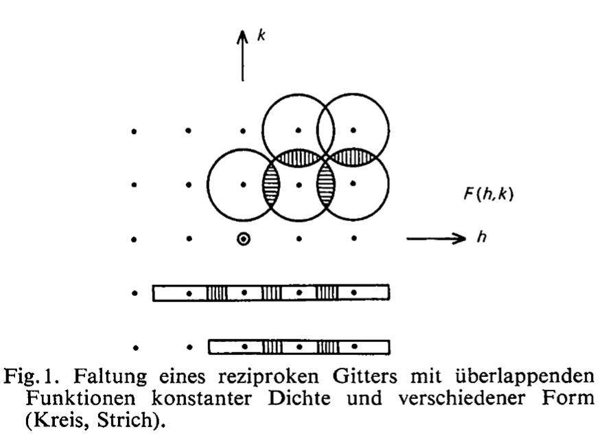
Ptychography: The origins

  • The diffraction signal in STEM contains the phase information of the sample

\[ T(\vec{r}) = \exp^{i \sigma V(\vec{r})} \]

  • The phase shift \(\sigma\) is related to the potential \(V(\vec{r})\) of the sample

  • Question: How can we measure the phase shifts of a sample in the STEM?

“In the case of inorganic crystals, and perhaps also in the case of radiation-sensitive organic crystals, these procedures could easily
develop into being competitors for the methods described in Sections 2.3-2.10 (CTEM, Zone plates)” [1]

Adapted from Hoppe (1983) Fig. 1: convolution of a reciprocal lattice with overlapping probe functions (circle, line).
Walter Hoppe [2]

Reciprocity & parallax — the tcBF equations

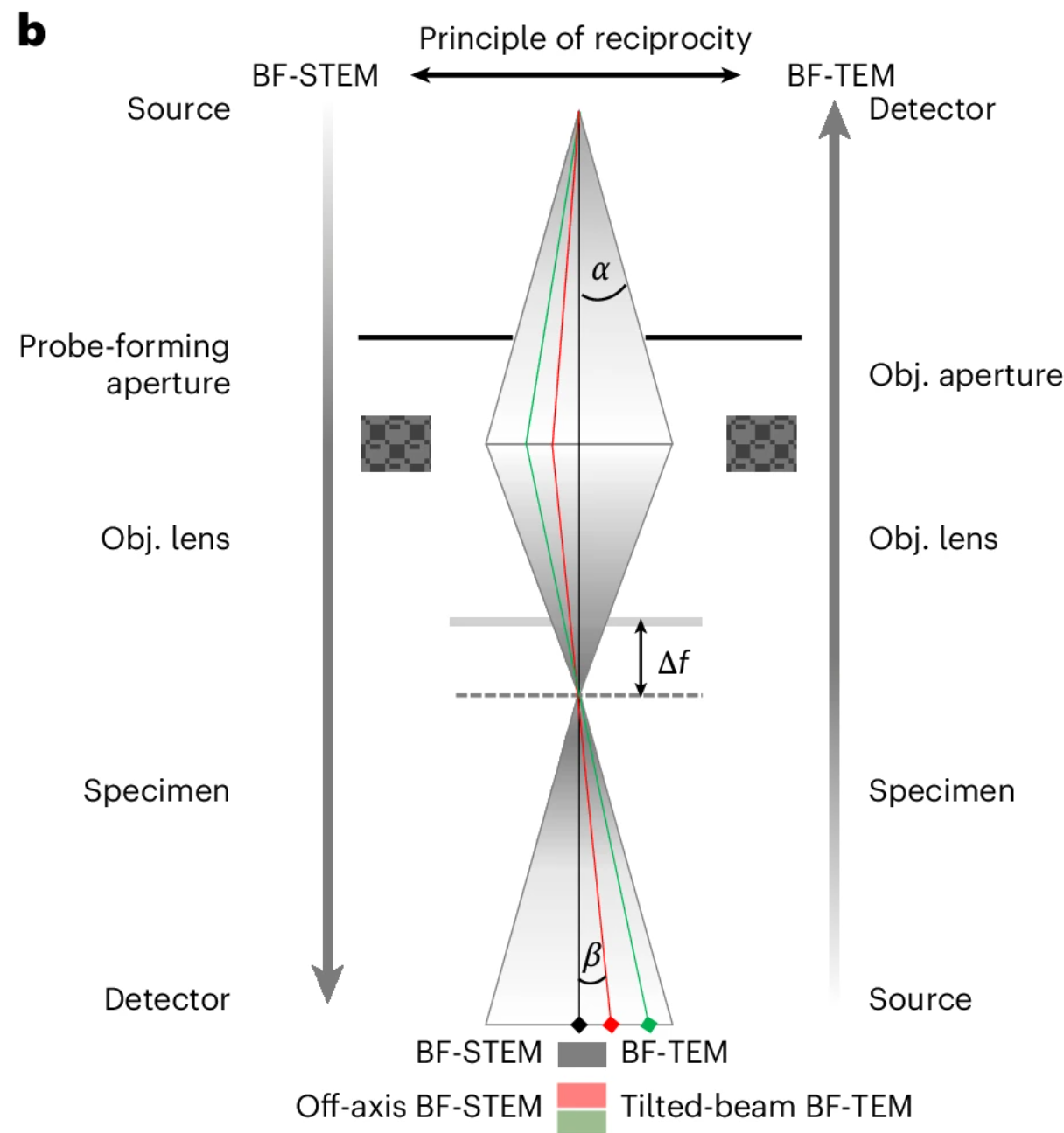
By reciprocity, every bright-field detector pixel is a tilted plane-wave view of the sample; defocus and aberrations then shift those views by a measurable parallax.

Reciprocity → virtual bright fields

  • A detector pixel at \(\mathbf{k}\) inside the BF disk is illumination tilted by \[ \boldsymbol{\theta}(\mathbf{k}) = \lambda\,\mathbf{k} \]
  • A virtual bright-field (VBF) image is that single pixel scanned over probe positions \(\mathbf{R}\): \[ I_{\mathbf{k}}(\mathbf{R}) \equiv I(\mathbf{R}, \mathbf{k}) \]
  • → one tilted-illumination image of the object per BF pixel.

Adapted from Yu et al. (2025) Fig. 1b: reciprocity — each off-axis BF-STEM pixel (top-down) equals a tilted-illumination BF-TEM view (bottom-up); defocus \(\Delta f\) introduces phase contrast.

Note

A real-space shift \(\mathbf{s} = \tfrac{1}{2\pi}\nabla_{\mathbf{k}}\chi\) is a reciprocal-space phase ramp \(e^{\,i\,\nabla_{\mathbf{k}}\chi(\mathbf{k})\cdot\mathbf{Q}_p}\)

Virtual Bright Fields and Parallax

Note

Each bright-field detector pixel is one illumination tilt (reciprocity), \(\boldsymbol{\theta} = \lambda\mathbf{k}\). Defocus × tilt → lateral parallax shift \(\mathbf{s}(\mathbf{k}) = \lambda\,\Delta f\,\mathbf{k}\) in the virtual image.

Correcting Aberrations: tcBF / Parallax Imaging

Note

Match the aberration surface → realign the virtual-BF stack → sharpen. Parallax/tcBF is the fast quadratic approximation to full SSB inversion.

Direct Phase Retrieval: One Forward Model, Many Acronyms

Under the weak phase object approximation, \(G(\mathbf{Q}_p, \mathbf{K}_f) = \hat{W}(\mathbf{Q}_p, \mathbf{K}_f)\,\tilde{\varphi}(\mathbf{Q}_p) + n\) — all linear estimators differ only in weighting and normalization (Varnavides et al. 2026).

Method Also known as Kernel / approximation Normalization
SSB acBF ptychography full \(\hat{W}\), one sideband none
OBF optimum bright field full \(\hat{W}\) RMS overlap (noise flattening)
MF / WDD matched filter / Wigner deconv. full \(\hat{W}\) (mixed domain) Wiener / LS
Parallax tcBF STEM \(\exp[i\nabla_k \chi(k)\cdot \mathbf{Q}_p]\) only phase flip + sum
iCOM / iDPC integrated CoM first moment \(\int \hat{W}\,\mathbf{k}\,d\mathbf{k}\) Fourier integration

Note

Direct methods: ms reconstruction → live feedback during acquisition and initial guesses for iterative engines

SSB / acBF Ptychography

Phase-compensated coherent sum over the aperture-overlap kernel \(\hat{W}(\mathbf{Q}_p, \mathbf{K}_f) = \tilde{\psi}^*(\mathbf{K}_f)\tilde{\psi}(\mathbf{K}_f - \mathbf{Q}_p) - \tilde{\psi}(\mathbf{K}_f)\tilde{\psi}^*(\mathbf{K}_f + \mathbf{Q}_p)\):

\[ \tilde{\varphi}_\mathrm{SSB}(\mathbf{Q}_p) = \sum_{\mathbf{K}_f \in \mathrm{double\text{-}overlap}} \hat{W}^*(\mathbf{Q}_p, \mathbf{K}_f)\, G(\mathbf{Q}_p, \mathbf{K}_f)\, \big/ |\hat{W}(\mathbf{Q}_p, \mathbf{K}_f)| \]

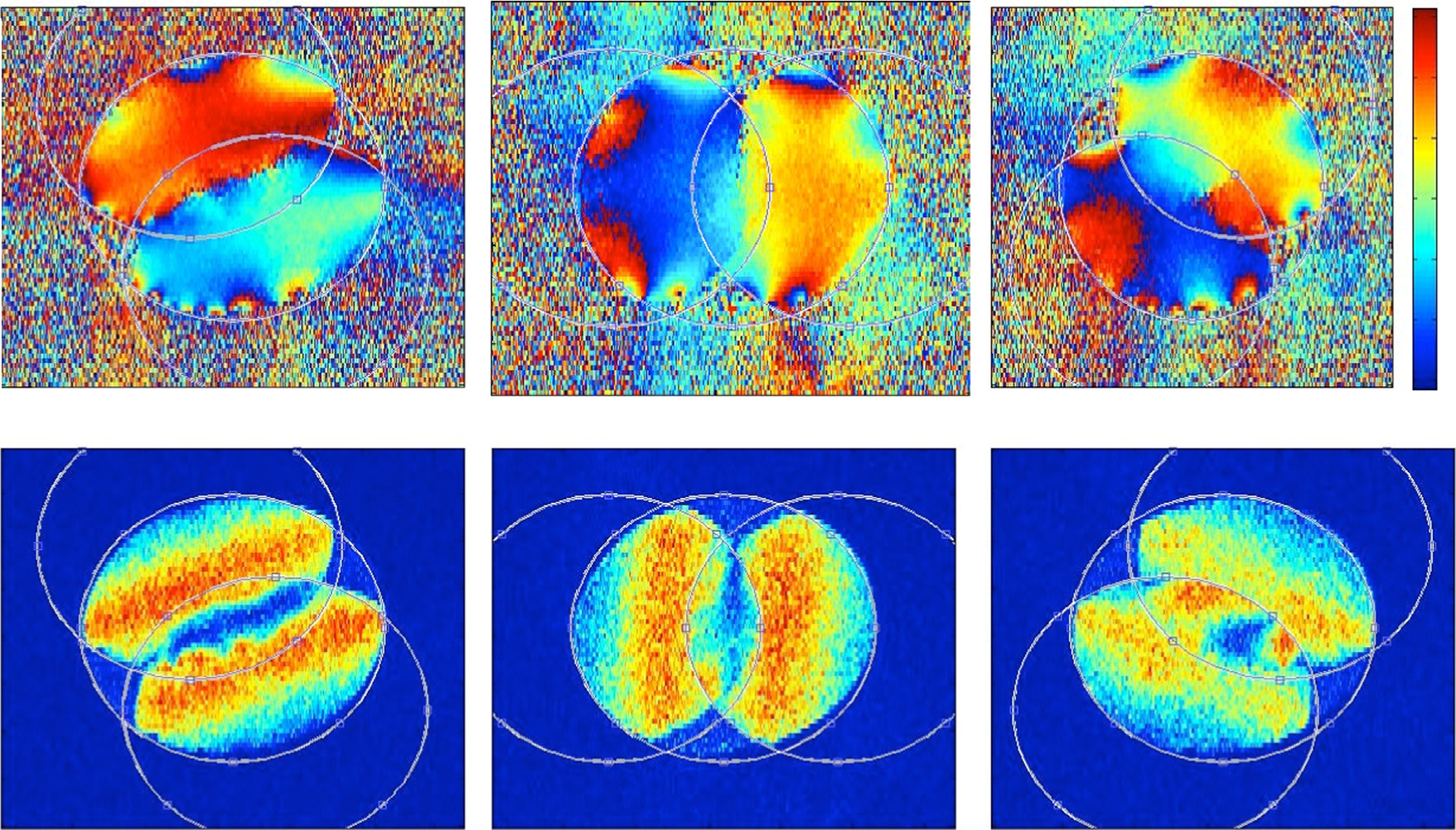
Sideband structure in \(G(\mathbf{K}_f, \mathbf{Q}_p)\) for graphene (Pennycook et al. 2015).

Note

SSB uses only the double-overlap (single sideband); beyond \(|Q| > q_0\) the CTF collapses to the ideal aperture autocorrelation envelope (Yang et al. 2016).

Deconvolution Interactive

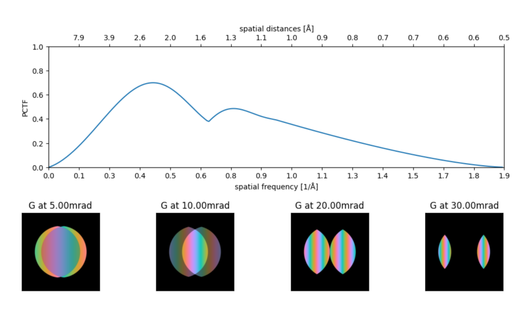
Analytical Theory and Contrast Transfer

  • The phase contrast transfer function (PCTF) describes how specimen spatial frequencies are transferred
  • For SSB under the WPOA:

\[ \mathrm{PCTF}_\mathrm{SSB}(\mathbf{Q}_p) = \frac{i}{2}\sum_{\mathbf{K}_f} |\hat{W}(\mathbf{Q}_p, \mathbf{K}_f)| \]

  • \(\hat{W}\) uses the full complex probe \(\tilde{\psi}(\mathbf{K}_f) = A(\mathbf{K}_f)\,e^{-i\chi(\mathbf{K}_f)}\) — aberration phase is built in
  • CTF sets the maximum transferable signal; SSNR / DQE quantify what is statistically reliable (Varnavides et al. 2026)
  • Optimal transfer: \(\mathrm{PCTF} = 1\)
  • Reduced transfer when direct and scattered beams do not overlap constructively
  • Axial BF (\(\mathbf{K}_f = 0\)): \(\mathrm{PCTF} \propto -i\sin[\chi(\mathbf{Q}_p)]\) — the HRTEM reciprocity link

Note

Tune convergence angle and defocus to maximize phase contrast at the spatial frequencies you care about

Analytical Theory and Contrast Transfer: Visual

Beyond the Weak Phase Object: When to Go Iterative

  • Direct BF ptychography is self-linearizing for moderate phase: even-order Born terms populate an absorptive channel suppressed by phase-selective operators
  • Direct methods excel at low dose and live feedback; iterative methods win for thick / strongly scattering samples
  • First ePIE iteration ≈ SSB deconvolution; later iterations extend the effective CTF toward unity
  • Projection-set: ER, DM, RAAR — robust, no explicit loss function
  • Gradient-based: ePIE → SGD/Adam — interfaces with autodiff, multislice, mixed-state, learned priors

Note

Workflow: fast direct reconstruction during acquisition → offline iterative / multislice on GPU

Part 3 · The 4D-STEM acquisition chain

Pixelated detectors deliver enormous data rates. How do we acquire, store, and preview 4D-STEM in practice?

1 · X-ray vs e⁻
2 · Phase & direct
3 · Acquisition
4 · Iterative & 3D
5 · Fields

Detector Evolution: Hybrid Pixel Array Detectors

  • Thick high-Z sensor + per-pixel electronics (counting, thresholds)
  • EMPAD (Tate et al. 2016): 128×128, 1.1 kHz, dynamic range ~1:1,000,000 → records the full bright-field disk and single electrons in the same pattern
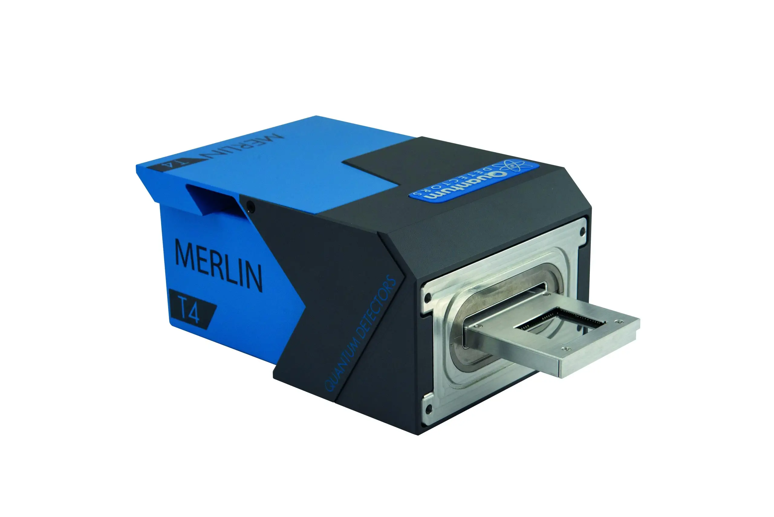
  • Medipix3 / Merlin (Ballabriga et al. 2013): 256×256 counting, 12/24-bit, up to ~kHz frame rates
  • Trade-offs:
    • modest pixel counts (128–512)²
    • thick sensor → charge sharing between pixels at high energy
    • radiation-hard, tolerate direct central beam

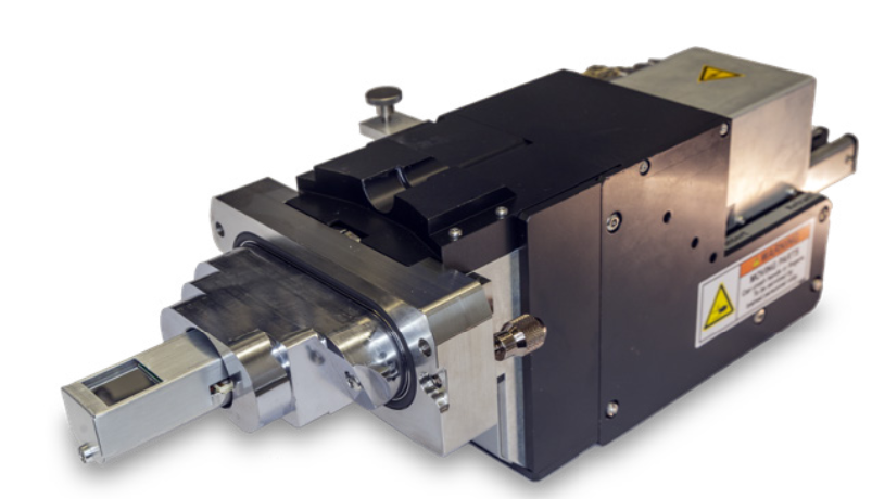
EMPAD pixel array detector

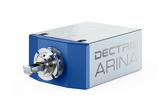
DECTRIS ARINA detector

Note

Hybrid PADs are the current workhorses for ptychography: high dynamic range where the central beam lives

Detector Evolution: Event-Driven Detection

  • Timepix3 (Poikela et al. 2014) / Timepix4 (Llopart et al. 2022): no frames — each electron is an event (x, y, time-of-arrival, time-over-threshold)
  • Time resolution ~1.6 ns; sparse readout → data volume scales with dose, not with scan size
  • Demonstrated 4D-STEM with µs dwell times (Jannis et al. 2022)
  • Consequences:
    • dwell time becomes a free post-processing choice (re-binning events in time)
    • natural fit for low-dose & in-situ experiments
    • needs new sparse data formats and event-based algorithms

Timepix4 event-driven detector

Note

Event-driven cameras dissolve the concept of “frame rate” — acquisition speed is set by the scan, not the camera

Data Rates: Drinking from the Firehose

  • 4D-STEM multiplies data: (scan pixels) × (detector pixels)
  • Merlin @ 4 kHz, 256², 12-bit → ~3 Gbit/s
  • 4D Camera @ 87 kHz, 576×576 → ~480 Gbit/s, ~700 GB per minute (Ercius et al. 2024)
  • A single overview scan (2k×2k probe positions) with a 256² camera = 0.5 TB raw
  • Survival strategies:
    • electron counting + sparse/compressed formats (events, run-length encoding)
    • hierarchical formats: HDF5 / EMD, vendor formats (.mib, .dm5)
    • keep raw data close to GPUs — network becomes part of the microscope

Note

Budget storage and compute per session, not per project — TB/day is normal now

Part 4 · Iterative & multislice 3D imaging

Real specimens are thick and the inverse problem has many knobs. How do iterative reconstruction and multislice tomography fit together?

1 · X-ray vs e⁻
2 · Phase & direct
3 · Acquisition
4 · Iterative & 3D
5 · Fields

Bayesian Framework for Inverse Problems

  • Goal: Estimate unknown image \(\mathbf{x}\) from a diffraction pattern amplitude \(\mathbf{y}\)
  • \(p(\mathbf{x} | \mathbf{y})\): posterior probability of the unknown image given the diffraction pattern
  • The most likely image, given the measurements:

\[\boxed{\hat{\mathbf{x}} = \arg\min_{\mathbf{x}} -\log p(\mathbf{y}|\mathbf{x}) - \log p(\mathbf{x})}\]

\[\begin{align*} \hat{\mathbf{x}} &= \arg\max_{\mathbf{x}} p(\mathbf{x}|\mathbf{y}) \\ &\overset{(i)}{=} \arg\max_{\mathbf{x}} \frac{p(\mathbf{y}|\mathbf{x})p(\mathbf{x})}{p(\mathbf{y})} \\ &\overset{(ii)}{=} \arg\max_{\mathbf{x}} p(\mathbf{y}|\mathbf{x})p(\mathbf{x}) \\ &\overset{(iii)}{=} \arg\max_{\mathbf{x}} \log\left(p(\mathbf{y}|\mathbf{x})p(\mathbf{x})\right) \\ &= \arg\min_{\mathbf{x}} -\log p(\mathbf{y}|\mathbf{x}) - \log p(\mathbf{x}). \end{align*}\]
    1. Bayes’ rule: \(p(\mathbf{x} | \mathbf{y}) = \dfrac{p(\mathbf{y} | \mathbf{x})\, p(\mathbf{x})}{p(\mathbf{y})}\)
    1. \(p(\mathbf{y})\) does not depend on \(\mathbf{x}\)
    1. The log-likelihood increases monotonically

Note

Many modern ptychography algorithms use a Bayesian framework

Bayesian Framework for Ptychography

The likelihood for a linear forward model with Gaussian noise is:

\[ p(\mathbf{y}|\mathbf{x}) \sim \exp\left(-\frac{1}{2\sigma^2} \|\mathbf{P}(\mathbf{x}) - \mathbf{y}\|_2^2\right) \]

where \(\mathbf{P}\) is the ptychography measurement operator, \(\mathbf{x}\) is the unknown image, \(\mathbf{y}\) is the measured data, and \(\sigma^2\) is the noise variance. The negative log-likelihood for a forward model with Gaussian noise is:

\[ -\log p(\mathbf{y}|\mathbf{x}) = \frac{1}{2\sigma^2} \|\mathbf{P}(\mathbf{x}) - \mathbf{y}\|_2^2 + c \] The prior term \(-\log p(\mathbf{x})\) is often called the regularization in optimization. It can be written as: \[ \lambda \sigma^2 \mathcal{R}(\mathbf{x}) = -\log p(\mathbf{x}) \] where \(\mathcal{R}(\mathbf{x})\) is a regularization function (e.g., enforcing smoothness or sparsity), \(\lambda\) is a regularization parameter, and \(\sigma^2\) is the noise variance. The resulting optimization problem for MAP estimation in the case of a linear forward model and Gaussian noise is:

\[ \hat{\mathbf{x}} = \arg\min_{\mathbf{x}} \frac{1}{2} \|\mathbf{P}(\mathbf{x}) - \mathbf{y}\|_2^2 + \lambda \mathcal{R}(\mathbf{x}) \]

where

  • \(\mathbf{P}(\mathbf{x})\) is the measurement operator,

  • \(\mathbf{y}\) is the measured data,

  • \(\mathcal{R}(\mathbf{x})\) is the regularization (prior) term, and

  • \(\lambda\) controls the strength of the regularization.

  • first term enforces data fidelity

  • second term encodes prior knowledge or constraints on the solution (regularization)

Iterative Reconstruction Methods: Basic Ptychography Algorithm

Code
import torch
import torch.fft as fft
from torch import Tensor
import skimage.data as skdata  
import skimage.transform as sktrans
import matplotlib.pyplot as plt
from scipy.ndimage import gaussian_filter
import numpy as np
img = skdata.astronaut()

img = sktrans.resize(img, (64, 64))
img = gaussian_filter(img, sigma=1)
# Convert to grayscale by taking mean across color channels
img = np.mean(img, axis=2)
img = img.astype(np.float32) / 255.0
img = torch.from_numpy(img)  
complex_image = torch.polar(torch.ones_like(img), img/img.max()*0.4)

Ingredient 1: scanning over the sample

def C(image : Tensor, positions : Tensor, window_size : int) -> Tensor:
    # Cropping operator: crop windows from the image at the given positions
    scan_windows = [] 
    for i, (x, y) in enumerate(positions):
        x_indices = torch.arange(x, x + window_size) % image.shape[1]
        y_indices = torch.arange(y, y + window_size) % image.shape[0] 
        Y, X = torch.meshgrid(y_indices, x_indices, indexing='ij') 
        window = image[Y, X]
        scan_windows.append(window)        
    scan_windows = torch.stack(scan_windows, dim=0)
    return scan_windows

Ingredient 2: propagation / interference

def F(wave):
  return fft.fft2(wave)

Simplest Ptychography Model

\[P(\mathbf{x}, \mathbf{\psi}, \mathbf{\rho}) = \left| \mathcal{F} \left( \mathbf{\psi(r)} \cdot \mathbf{C}(\mathbf{x}, \mathbf{\rho}) \right) \right|\]

def P(sample, probe, scan_positions):
  # crop the scanning windows, transmit the beam, propagate 
  # to detector, then detect
  return th.abs(F(probe * C(sample, scan_positions, probe.shape[0])))
Code
import numpy as np
import plotly.graph_objects as go
import plotly.io as pio

# Configure plotly for both VS Code and Quarto rendering
pio.renderers.default = "plotly_mimetype+notebook_connected"

# Define scan grid
size = 8
step = 1
x = torch.arange(0, size, step)
y = torch.arange(0, size, step)
X, Y = torch.meshgrid(x, y, indexing='ij')
positions = torch.stack([X.flatten(), Y.flatten()], dim=1)  # Kx2 array
K = positions.shape[0]

# Example sample image (replace with your own)
sample = complex_image

# Example probe (window size)
probe_size = 32 
probe = torch.ones((probe_size, probe_size))

# Crop image stack
image_stack = C(sample, positions, probe_size)  # shape: (K, probe_size, probe_size)

# Create interactive plotly figure with title "scanning windows"
fig = go.Figure()
# Add initial image
fig.add_trace(go.Heatmap(
    z=np.angle(image_stack[0].detach().cpu().numpy()),
    colorscale='inferno',
    showscale=False
))
# Add slider, set black background, add figure title, and set text color to white
fig.update_layout(
    title=dict(text="Scanning Windows", font=dict(color='white')),
    width=400,
    height=500,
    margin=dict(l=0, r=0, t=40, b=0),
    xaxis=dict(showticklabels=False, showgrid=False, color='white', title_font=dict(color='white')),
    yaxis=dict(showticklabels=False, showgrid=False, color='white', title_font=dict(color='white')),
    sliders=[dict(
        active=0,
        currentvalue={"prefix": "Position: ", "font": {"color": "white"}},
        len=0.9,
        x=0.1,
        xanchor="left",
        y=0,
        yanchor="top",
        steps=[dict(
            method="restyle",
            args=[{"z": [np.angle(image_stack[i].detach().cpu().numpy())]}, [0]],
            label=str(i)
        ) for i in range(K)],
        font=dict(color='white')
    )],
    paper_bgcolor='black',
    plot_bgcolor='black',
    font=dict(color='white')
)
fig.show()

Experimental Design Considerations: parameter flexibility

Adjustable parameters for ptychographic data acquisition [1]
Limitation/check Description Default
Areal oversampling How many probes illuminate each pixel?
\[A = \frac{\pi r_p^2}{s^2}\]
1.6 - 1e3
Probe sampling To which extent is the probe contained in its window?
\[P = \frac{1}{2r_pd}\]
< 0.5
Ronchigram magnification Size of the shadow image on the detector plane in units \(\frac{pixel}{Å}\)
\[M = \frac{\alpha}{\theta \cdot r_p} = \frac{\alpha}{\lambda d \cdot r_p}\]
10 - 100

where:

  • \(\alpha\) is the semi-convergence angle
  • \(\theta\) is the angular sampling in radians
  • \(s\) is the scan step size
  • \(r_p\) is the probe radius
  • \(d\) is the diffraction space sampling

Experimental Design Considerations: sampling

Note

sampling in diffraction space & defocus → Ronchigram Magnification

sampling in real space & defocus → Areal oversampling

Modeling partial coherence

  • partial coherence arises from multiple sources in electron microscopy:
    • finite source size –> partial spatial coherence of the electron source [1]
    • finite detector pixel size –> partial spatial coherence
    • finite energy spread inside the column –> partial temporal coherence [1]
  • most efficient models:
    • detector pixel size & source size: convolution in the detector plane [2]
    • energy spread & remaining partial coherence: multiple coherent modes [3]

\[ I(\vec{\rho}, \vec{q}) =\left(\color{red}{\sum_n a_n} \left|\mathcal{F}\left[O(\vec{\vec{r}})\color{red}{\psi_n(\vec{r}-\vec{\rho})}\right]\right|^2\right) \color{green}{\otimes M(\vec{q})} \]

where:

  • \(\vec{\rho}\) is the position on the detector plane
  • \(\vec{q}\) is the position in reciprocal space
  • \(a_n\) is the amplitude of the \(n\)-th coherent mode
  • \(O(\vec{r})\) is the aperture function
  • \(\psi_n(\vec{r}-\vec{\rho})\) is the wave function of the \(n\)-th coherent mode, shifted by the position \(\vec{\rho}\)
  • \(M(\vec{q})\) is the a function modeling modulation transfer function and partial source coherence

Experimental Design Considerations: coherence

Note

temporal coherence is no problem at 200-300kV, ~2-3 modes

at low energies 30-60keV, temporal coherence needs more modes

superresolution capabilities circumvent the coherence problem

Adding more “nuisance parameters”: Refining the scan positions

  • realistic model for thin samples:

\[ P(\mathbf{x}, \mathbf{\psi}, \mathbf{\rho}) = \left|\left(\sum_n a_n \left|\mathcal{F}\left[O(\vec{\vec{r}})\psi_n(\vec{r}-\vec{\rho})\right]\right|^2\right) \otimes M(\vec{q})\right| \]

\[ \hat{\mathbf{x}} = \arg\min_{\color{red}{\mathbf{x}, \mathbf{\psi}, \mathbf{\rho}}} \frac{1}{2} \|P(\mathbf{x}, \mathbf{\psi}, \mathbf{\rho}) - \mathbf{y}\|_2^2 + \lambda \mathcal{R}(\mathbf{x}) + \lambda_1 \mathcal{R}_1(\mathbf{\psi}) \]

Note

modern ML frameworks allow us to refine additional parameters easily using automatic gradient calculations

Modeling thick samples: the multi-slice algorithm

  • Up to now: thin samples, i.e. thickness < depth of field and weak scattering
  • Thick samples require modeling of multiple scattering events
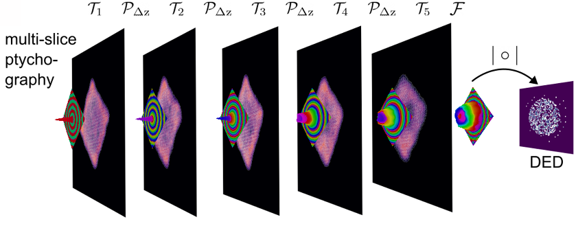
  • Sample is divided into thin slices that can be treated independently
  • Beam propagates through slices sequentially

Multi-slice propagation model (Adapted from [1])

\[\psi_{n+1}(r) = \mathcal{P}_{\Delta z} \left[ t_n(r) \psi_n(r) \right]\]

where:

  • \(\psi_n(r)\) is the wave at slice n
  • \(t_n(r)\) is the transmission function
  • \(\mathcal{P}_{\Delta z}\) is the propagator (usually Fresnel)
  • \(\Delta z\) is the slice thickness

Key parameters:

  • Slice thickness (typically 1-2 nm)
  • Number of slices
  • Propagation distance

Multi-slice ptychography (MSP)

Component Mathematical Description
Multislice algorithm \[\mathcal{M}_{\psi}(\mathbf{V}) = \prod_{k=0}^T (\mathcal{P}^{\Delta z} T^{\mathbf{V}_k})\psi \]
Multi-slice ptychography model \[P(\mathbf{V}, \mathbf{\psi}, \mathbf{\rho}) = \left|\left(\color{red}{\sum_n a_n} \left|\mathcal{F}\left[\mathcal{M}_{\color{red}{\psi_n(\vec{r}-\vec{\rho})}}(\mathbf{V})\right]\right|^2\right) \color{green}{\otimes M(\vec{q})}\right|\]
Optimization problem \[\hat{\mathbf{V}} = \arg\min_{\mathbf{V}, \mathbf{\psi}, \mathbf{\rho}} \frac{1}{2} \|P(\mathbf{V}, \mathbf{\psi}, \mathbf{\rho}) - \mathbf{y}\|_2^2 + \lambda \mathcal{R}(\mathbf{V}) + \lambda_1 \mathcal{R}_1(\mathbf{\psi}) \]

Note

We have arrived at the state of the art in ptychography:

3D imaging with deep-sub-angstrom lateral and ~2nm depth resolution

Constraints in MSP: positive potential, amplitude~1, blur kernel

Constraint 1: Positive Potential

  • The electrostatic potential \(V(\mathbf{r})\) must be physically meaningful: \(V(\mathbf{r}) \geq 0\)
  • Enforced during optimization by projecting negative values to zero
  • Prevents unphysical solutions and improves stability

Constraint 2: Amplitude \(\approx 1\)

  • The transmission function \(t_n(\mathbf{r})\) should have amplitude close to 1 (very few electrons scattered outside the 4D-STEM detector are registered as “amplitude contrast”)
  • Enforced by regularization: penalize deviations from \(|t_n(\mathbf{r})| = 1\)

Constraint 3: Blur Kernel

  • in (x,y) plane: stabilize deep-sub-angstrom resolution reconstructions
  • in z-direction: limit depth resolution, disallow higher than 1nm depth resolution
  • early algorithms: Fourier-space convolution –> leads to wrap-around artefacts for non-periodic samples

Note

Minimal set of constraints to make the reconstruction stable.

Add your own flavour of constraints: more physics, data-driven priors, denoisers…

Extensions of MSP: mistilt correction

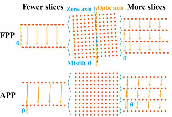
Slight misorientation of the zone axis can lead to stricter requirements for the slice thickness.
Solution: include the mistilt in the propagator, refine it during the reconstruction
Adapted from [1]

Adaptive propagator requires less slices
–> Faster reconstructions
Adapted from [1]

Note

Slight deviations from the perfect zone axis can be refined algorithmically

Extensions of MSP: atomistic models

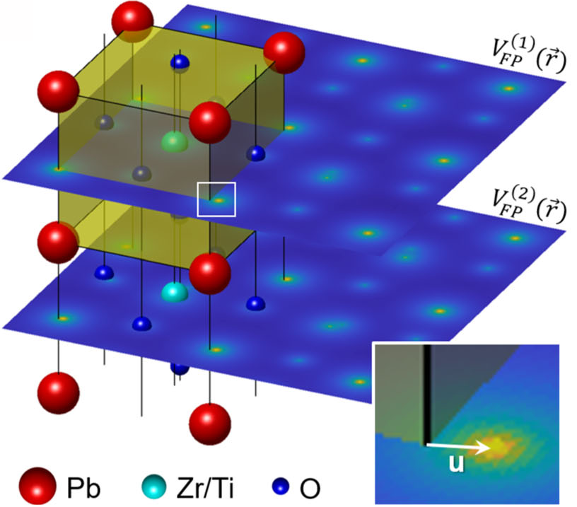
Assemble the electrostatic potential from atomic positions and atomic numbers

\[O_l(\mathbf{r}) = A_l(\mathbf{r}) e^{i \sigma_e V_{\mathrm{FP}}^{(j)}(\mathbf{r}, \boldsymbol{\tau})}\]

\[ V_{\mathrm{FP}}^{(j)}(\mathbf{r}, \boldsymbol{\tau}) = \sum_{n=1}^{N} w_n v_{Z_n} \left( \mathbf{r} - \mathbf{r}_n - \sqrt{\langle u_n^2 \rangle} \cdot \mathbf{g}_{n, \tau} \right) \]

Atomistic model for the reconstructed potential (Adapted from [2])

Note

Atomic positions can be refined directly

–> interpretable model, enables phonon modeling

–> sparse model –> achieves higher resolution than voxelized models

–> phonon modeling –> might enable imaging of phonon modes

Extensions of MSP: mixed-state objects & phonon correlations

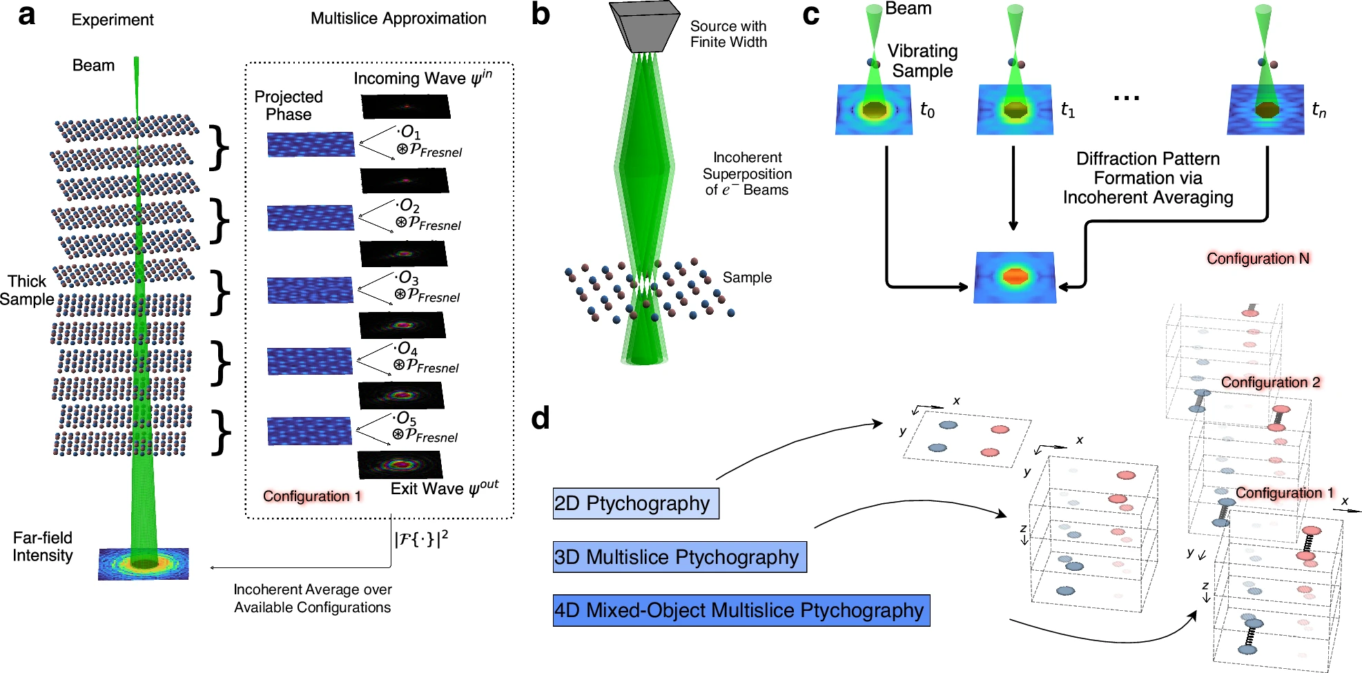
  • CAVIAR (Correlated Atomic Vibration Imaging with sub-Ångstrom Resolution): mixed-state multislice ptychography that retrieves interatomic displacement correlations
  • Forward model: incoherent sum over atomic configurations → diffraction intensities
  • Output: Green’s tensor of displacement correlations → phonon branches from few nm³ at room temperature

Adapted from [1]: Fig. 1 — multislice 4D-STEM simulation with multiple object configurations (phonon / thermal snapshots) summed incoherently to form each diffraction pattern.

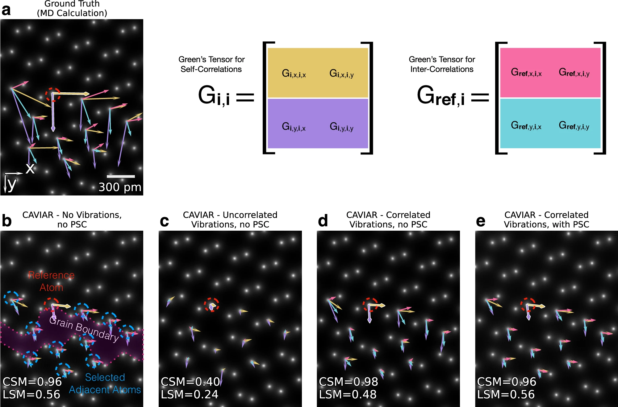
CAVIAR: simulated Σ9 Si grain boundary (Fig. 2)

Adapted from [1]: Ptychographic reconstructions for a symmetric Σ9 grain boundary in silicon — ground-truth MD correlations (a) vs. CAVIAR under no vibration, Einstein (uncorrelated), correlated vibrations, and partial spatial coherence (b–e). CSM/LSM quantify cosine- and length-similarity to ground truth.

Note

Correlated vibrations must be modeled explicitly; uncorrelated (Einstein) thermal motion destroys recovered interatomic correlations

CAVIAR: experimental hBN bicrystal (Fig. 3)

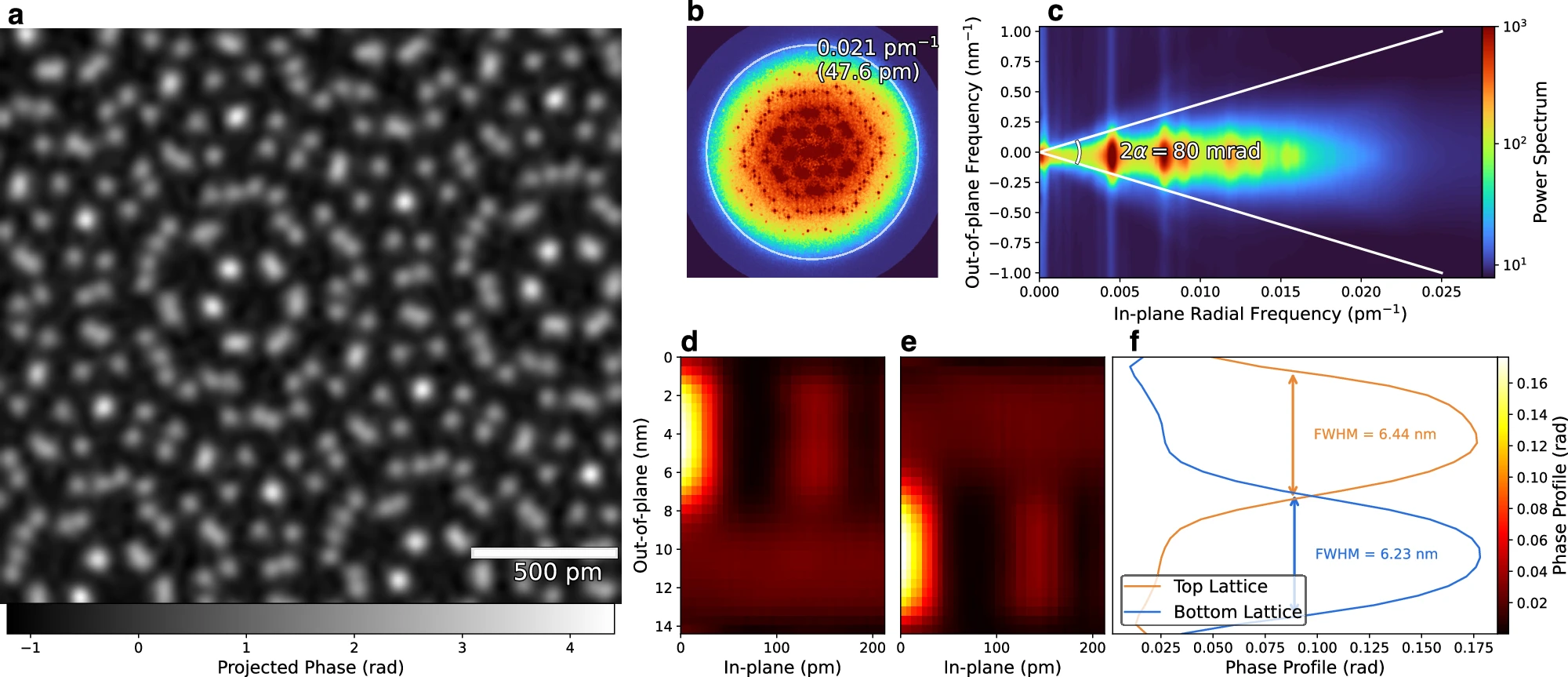
Adapted from [1]: ~15 nm hBN bicrystal (11° twist) reconstructed with 30 slices, 10 object states, 5 probe modes — projected phase (a), power spectrum to 47.8 pm (b), 3D Fourier cut-off (c), depth-resolved r–z phase maps separating upper/lower lattices (d–f).

Note

Mixed-state MSP resolves depth-separated lattices and extracts phonon-dispersion curves from displacement correlations — complementary to vibrational EELS

Applications of MSP: 3D imaging

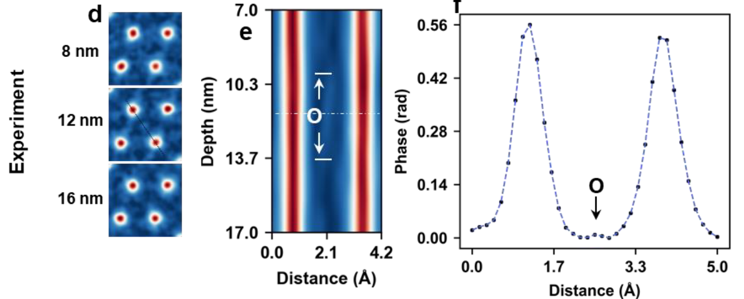
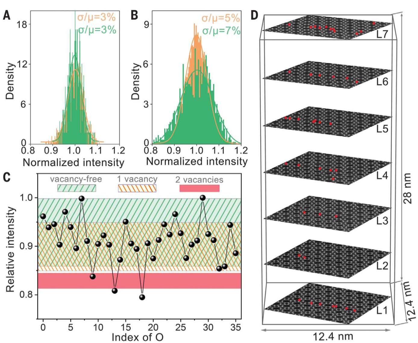
Adapted from [1]: Identification of O vacancies in ZSM-5. Intensity histograms and variations reveal O vacancies through comparison of experimental and simulated ptychographic phase images. Red dots in (D) show identified vacancy-containing columns across layers L1-L7.

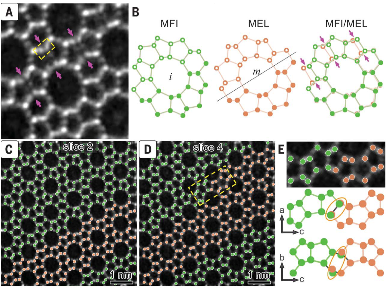
Adapted from [1]: (A) 4D-STEM ptychography image displaying extra T atoms (indicated by the magenta arrows) relative to the typical MFI framework. The yellow dashed rectangle indicates the region analyzed in Fig. 5A. (B) Structural projections of straight 10-MR channels of MFI and MEL and their superposition. The letters i and m denote inversion and mirror symmetry, respectively. (C and D) Second (C) and fourth (D) slices of the multislice ptychography reconstruction result.

Note

Excellent for imaging inhomogeneities of weakly scattering atoms

Applications of MSP: 3D imaging 2

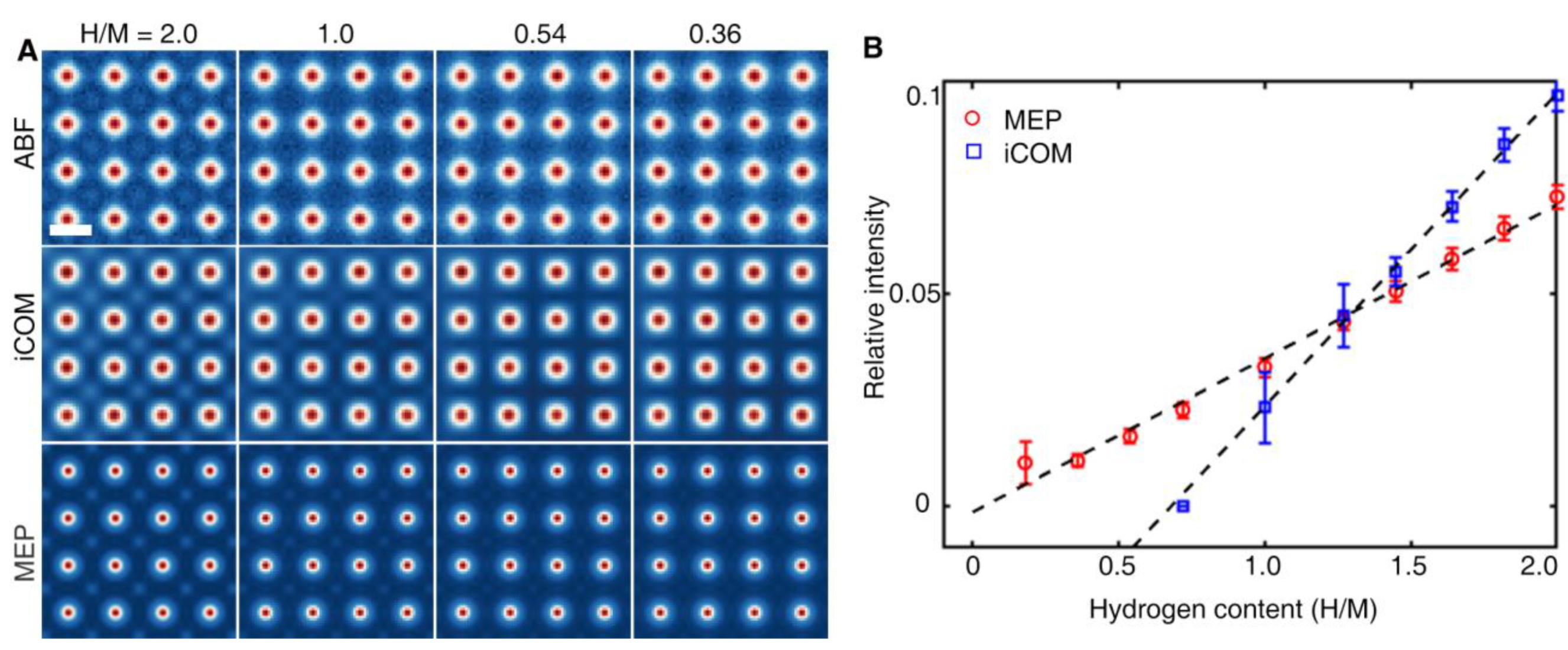
Adapted from [1]: Hydrogen detection sensitivity across different imaging techniques. (A) Simulated images of NbHx (15 nm thickness) with varying hydrogen content over Nb metal atoms (0.36-2.0 H/M) acquired by contrast-inverted annular bright-field (ABF), integrated center-of-mass (iCOM), and multislice electron ptychography (MEP). Scale bar, 2 Å. (B) Hydrogen-to-metal column intensities vs hydrogen content for iCOM and MEP, demonstrating MEP’s superior detection sensitivity.

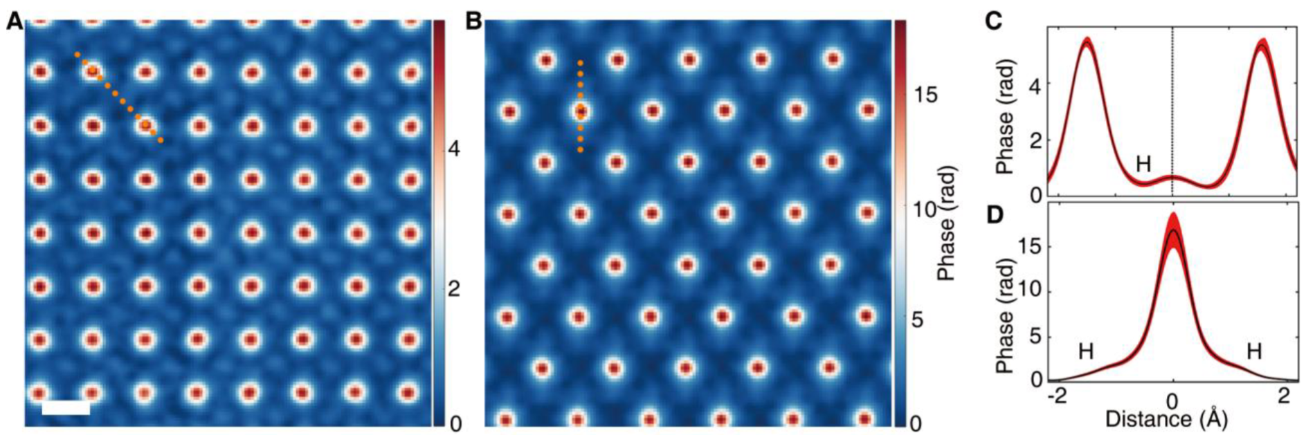
Adapted from [1]: TiH2 phase images along [100] and [110] zone axes using experimental data, summing middle slices (11-22 nm thickness)

Note

Even hydrogen columns can be resolved, if more than 4 H atoms.

Applications of MSP: ultra low-dose imaging

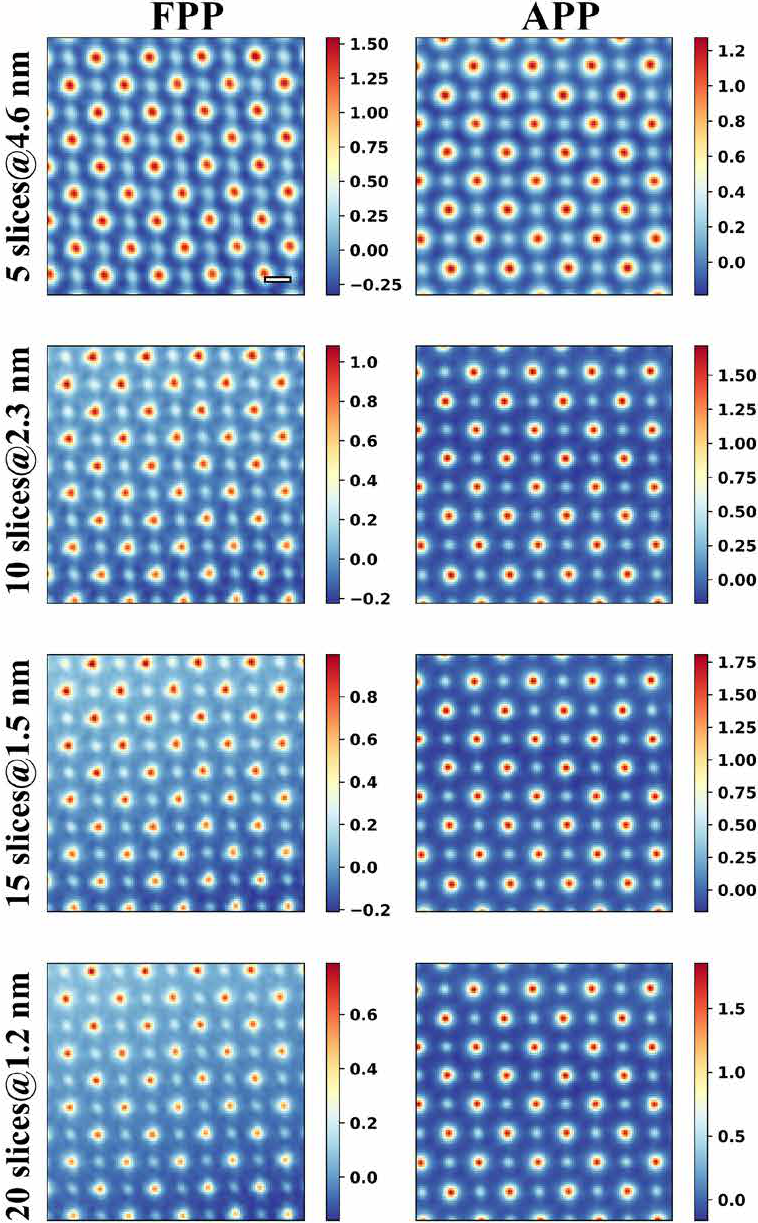
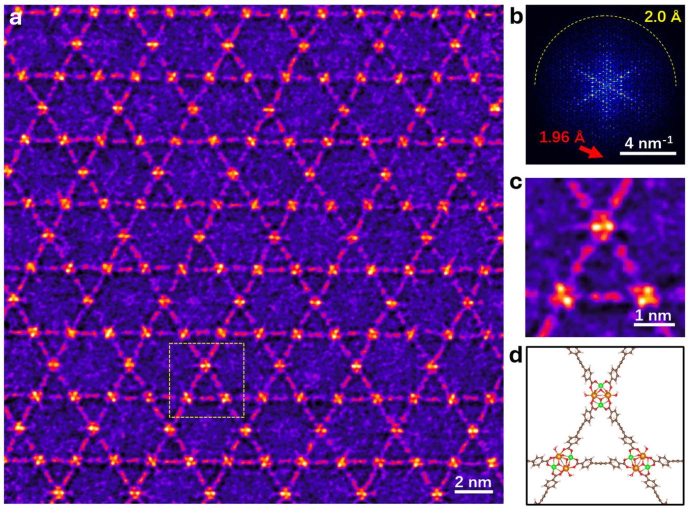
Adapted from [1]: MOF Zr-BTB imaged with electron ptychography at 115 e−/Å2 dose. (a) Phase image showing 2.25 Å resolution. (b-d) Power spectrum, enlarged region, and structural model showing excellent agreement.

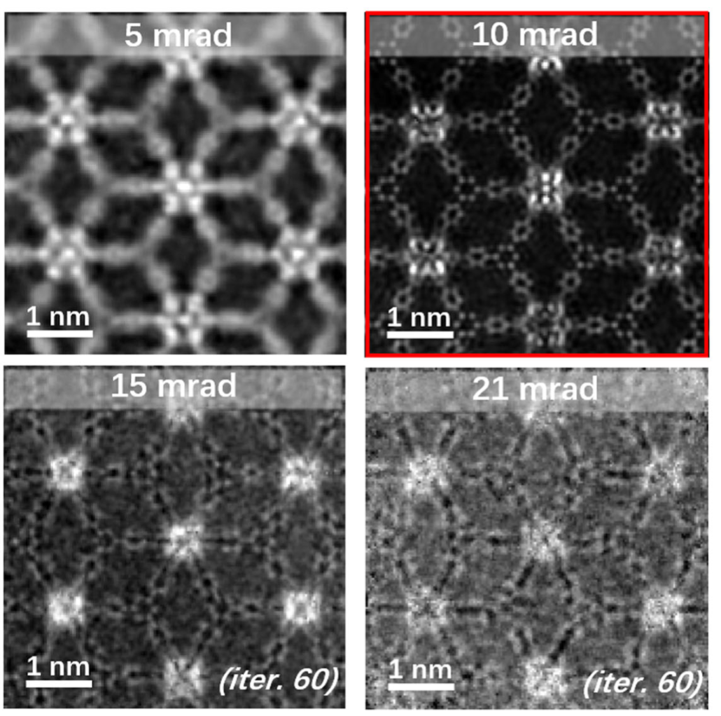
Adapted from [1]: Iterative reconstruction error curves (d) and reconstructed ptychography phase images (e) using 4D-STEM datasets simulated at varying convergence semiangles with a consistent electron dose of 100 e−/Å2. The 10-mrad case shows the best reconstruction, as marked by the red square.

Note

Multiple scattering from crystals at very low doses enables 2Šresolution at dosesof 100 e-/Ų

Limitations of MSP: axial resolution

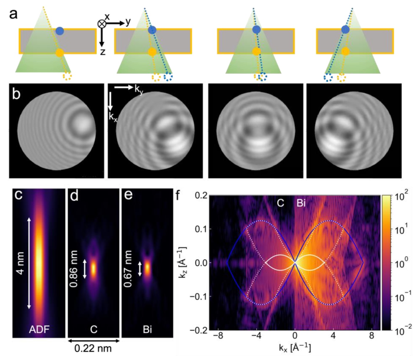
Adapted from [1]: Principle of depth sectioning via multislice electron ptychography

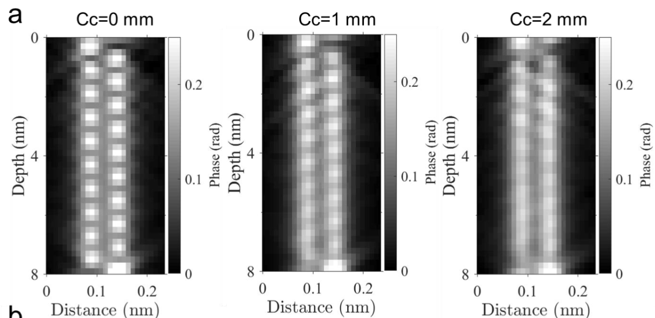
Adapted from [1]: Depth evolution of phase/intensity across Pr-Pr dumbbell showing strong dependence on chromatic aberration. Comparison between (a) multislice ptychography and (b) focal series ADF imaging.

Note

Axial resolution of MSP is (with current algorithms) limited to below atomic scale if not using the most cutting edge instrumentation

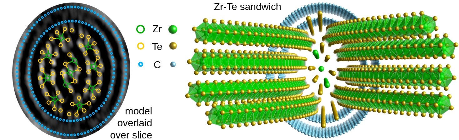
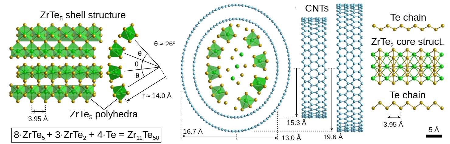
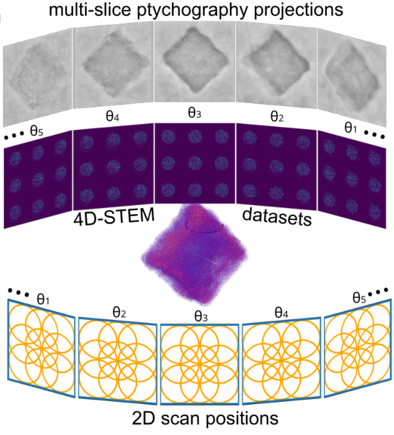
First unknown 3D atomic structure solved with 4D-STEM tomography

Approach:

  1. 4D-STEM tilt series
  2. mixed-state ptychography of all tilt angles

  1. Joint linear tomography and alignment
  2. Sub-pixel atomic peak tracing
  3. 3D atomic structure determination

Volume size: (6 nm)3

Note

Elliptic double-wall CNT and complex inner structure resolved in 3D

Full 3D: Single-Slice Ptychographic Tomography Solves Nanostructures

Note

First 3D atomic structure solved with phase-contrast tomography.
Novel ZrTe2 phase, confirmed stable with DFT simulations.

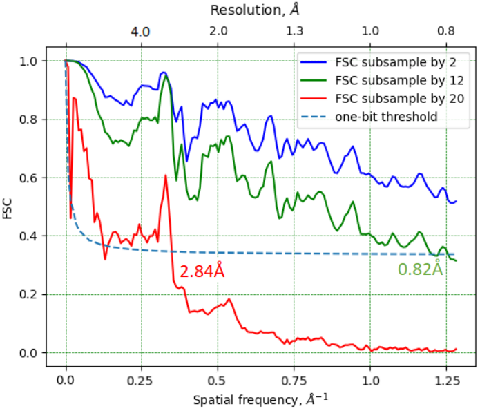
Depth Resolution Progress Over Time


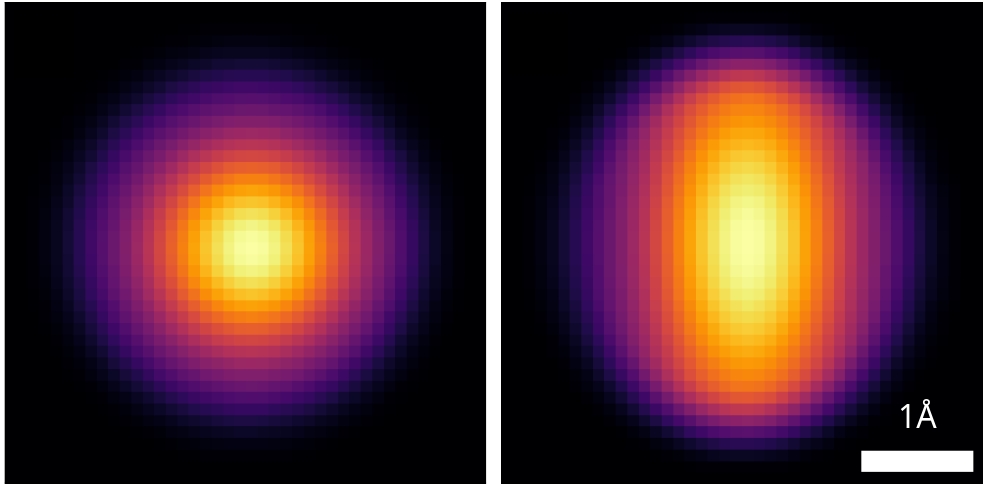
2022: 2.2 Å in 6nm thick volume using SSPT [1]

2023: 2.0 Å in 18nm thick volume using MSPT [2]

2024: 0.8 Å in 11nm thick volume using E2E-MSPT [3]

Note

Algorithm development drives resolution records and depth of focus enhancements

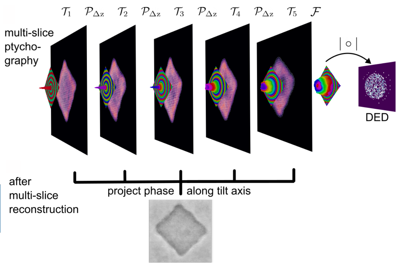
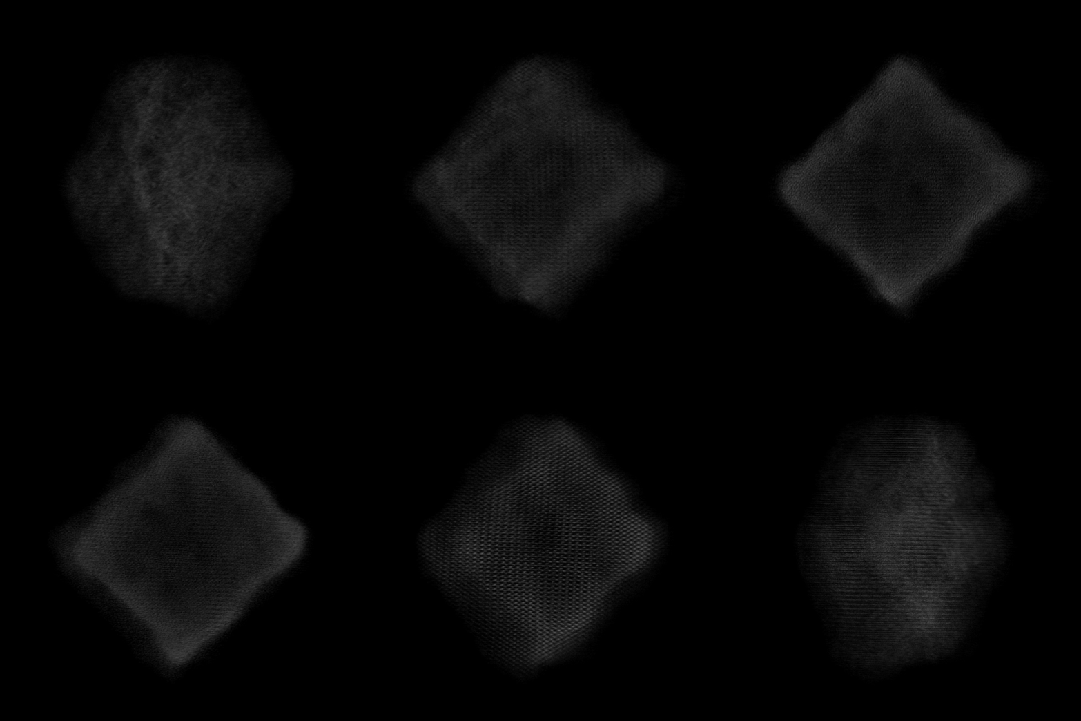
Full 3D: multis-slice ptychographic tomography

Perform MSP reconstruction
for each tilt angle
and project the potential along z


✅ Advantages:
- Decouple tomographic alignment from ptychographic reconstruction
- Can use positions and alignment as input to E2E-MSPT

Multi-slice Ptychographic Tomography forward model

❌ Disadvantage:
- Loses some 3D info from MSP

Joint Tomography and Rigid Alignment enables atomic resolution of beyond-DOF volumes

Note

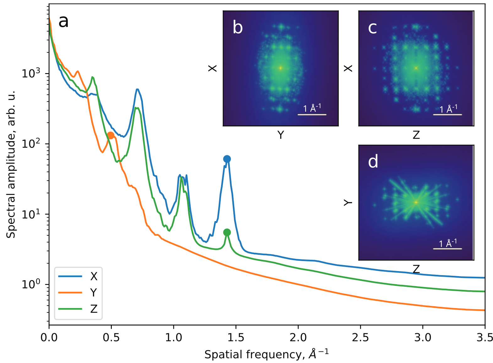
Enabled by reaching sub-pixel alignment at each scale

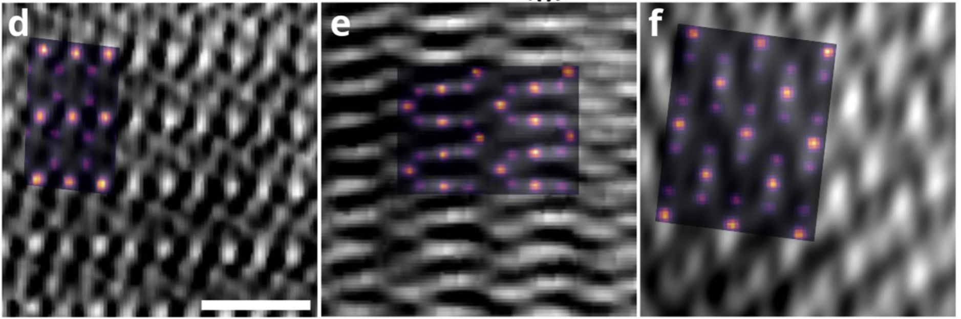
3x DOF volumes display atomic resolution

Note

Volume size: (18.2 nm)3 Voxel size: 0.3 Å

Orthoslices reveal lattice in all 3 dimensions

scale: 1 nm

Note

Lattice resolved, but Co atom contrast overpower O contrast
=> Around 1 Å z resolution required to resolve O atoms

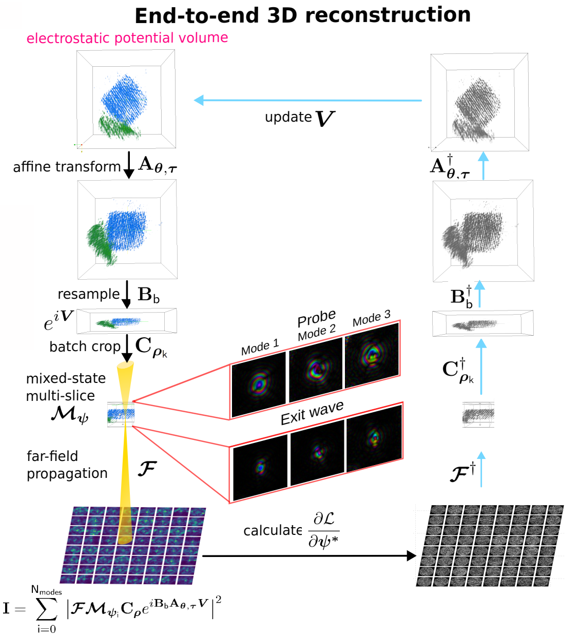
End-to-end reconstruction - putting all pieces together

Fully E2E-MSPT reconstruction includes

  1. affine resampling of potential volume
  2. z-resampling of potential volume (save compute)
  3. batch-croppping and mixed-state multi-slice model
  4. far-field propagation
  5. gradient backpropagation through full model

Note

The most accurate approximation for 4D-STEM tomography to-date

Part 5 · Fields, charge & magnetism

The reconstructed phase encodes more than atomic positions. Can we measure electric fields, charge transfer, and magnetism from the same 4D dataset?

1 · X-ray vs e⁻
2 · Phase & direct
3 · Acquisition
4 · Iterative & 3D
5 · Fields

From Structure to Fields: What Else Is in the Data?

  • So far: the object’s potential \(V(\vec{r})\) — atomic structure
  • The same 4D datasets encode more:

Electric fields \(\vec{E}(\vec{r})\) — deflection of the beam by the local field

Charge density \(\rho(\vec{r})\) — including valence redistribution due to bonding

Magnetic fields \(\vec{B}(\vec{r})\) — from textures (skyrmions) down to single atomic planes

Note

Fields are derivatives of the phase — everything we learned about phase retrieval carries over

Ptychography → Potential, Field, and Charge Density

  • Ptychography reconstructs \(O(\vec{r}) = e^{i\sigma V(\vec{r})}\) → phase ∝ projected electrostatic potential
  • Charge density from Poisson’s equation:

\[ \rho(\vec{r}) = -\varepsilon_0 \nabla^2 V(\vec{r}) \]

  • Uses all diffraction pixels dose-efficiently; post-corrects residual aberrations (Jiang et al. 2018; Hofer et al. 2025)
  • Subtract the independent-atom model (IAM) → valence redistribution from bonding
  • CoM/DPC gives \(\vec{E}_\perp\) directly from the first moment (Müller et al. 2014) — fast, but:
    • divergence amplifies noise; heavy regularization needed
    • residual aberrations can invert contrast and hide bonding-scale signals (Hofer et al. 2025)
  • Ptychographic phase is the route to quantitative charge transfer

Note

Bonding perturbs the charge density by ~10% at atomic sites — ptychography + aberration correction reaches the required precision

Why Ptychography for Charge Transfer?

  • Bonding-induced charge transfer is a small perturbation on the nuclear-dominated density
  • Prior CoM/DPC and holography reached atomic-resolution charge density but not bonding sensitivity (Hofer et al. 2025)
  • Residual lens aberrations can reverse W–S₂ dumbbell polarity → charge transfer invisible without correction
  • Focused-probe SSB ptychography (Hofer et al. 2025):
    • high-speed, dose-efficient 4D-STEM acquisition
    • simultaneous ADF for unambiguous structure/\(Z\)-contrast
    • post-collection aberration correction + parameter-based quantification
  • Interpretation requires quantitative simulations:
    • multislice 4D-STEM with DFT potentials (bonding included)
    • compare against IAM (bonding excluded)
    • thermal diffuse scattering from finite-\(T\) MD

Note

Ptychography supplies the measurement; DFT-based image simulation supplies the interpretation

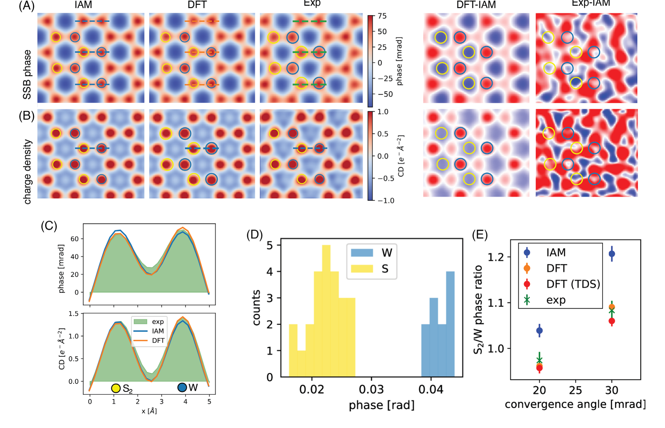
Charge Transfer in Pristine WS₂ (Fig. 2)

  • Monolayer WS₂: SSB phase and charge-density maps from experiment match DFT, not IAM (Hofer et al. 2025)
  • Bonding redistributes charge W → S:
    • higher phase/CD at W sites
    • reduced phase/CD at S₂ sites
  • Effect ≈ 10% of peak atomic signal — visible in DFT−IAM and Exp−IAM difference maps
  • \(S_2/W\) phase ratio: experiment agrees with DFT (+ TDS), IAM overestimates

Adapted from Hofer et al. (2025) Fig. 2: SSB phase and charge-density maps (IAM, DFT, experiment) for pristine WS₂; difference maps isolate bonding-induced charge transfer; line profiles and \(S_2/W\) phase-ratio quantification.

Note

Aberration-corrected ptychographic phase — not differentiated CoM — reaches the precision needed for bonding electrons

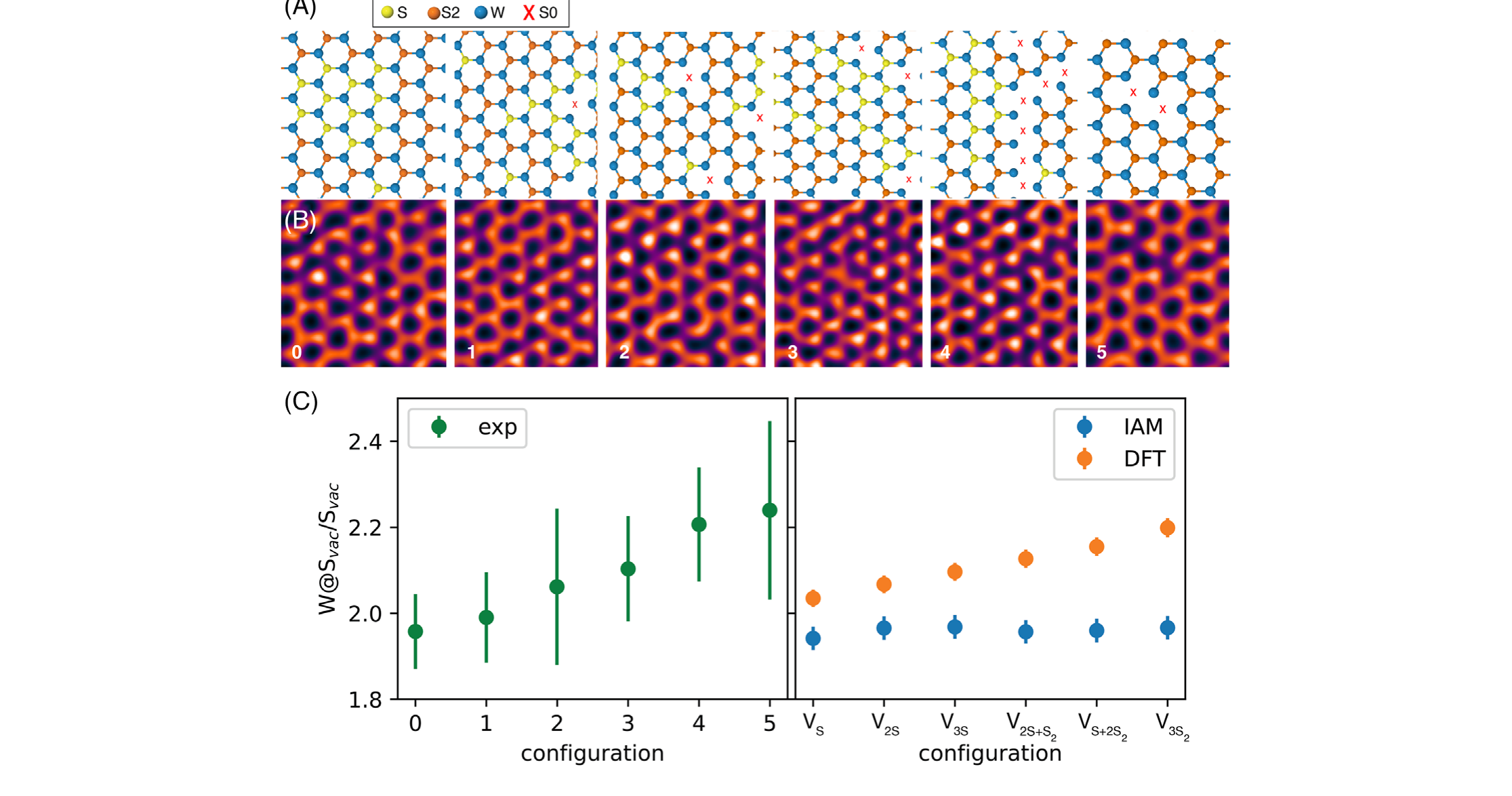
Charge Transfer at S Vacancies (Fig. 4)

  • Individual S monovacancies in WS₂: local charge environment changes with vacancy clustering (Hofer et al. 2025)
  • Metric: \(W@S_{\mathrm{vac}}/S_{\mathrm{vac}}\) phase ratio
    • increases with vacancy density in experiment
    • DFT simulations reproduce the trend
    • IAM predicts a flat ratio → misses charge transfer entirely
  • Defect charge transfer up to ~10% — requires site-averaging and low-dose-aware acquisition

Adapted from Hofer et al. (2025) Fig. 4: atomic models and SSB images of defective WS₂ with increasing S-vacancy density; experimental and simulated \(W@S_{\mathrm{vac}}/S_{\mathrm{vac}}\) phase ratio vs. defect configuration.

Note

Valence charge redistribution is detectable at defects, with ptychography matched to first-principles simulation.

Imaging Magnetic Fields: The Aharonov–Bohm Phase

  • The electron phase has an electrostatic and a magnetic part:

\[ \varphi(\vec{r}) = \sigma \int V \, dz \; - \; \frac{e}{\hbar} \int \vec{A} \cdot d\vec{l} \]

  • Magnetic phases are tiny: mrad per nm vs. rad for atomic potentials
  • Classic tools: Lorentz TEM, electron holography, segmented-detector DPC at low magnification
  • Challenges:
    • field-free objective lens (“Lorentz mode”) → poor conventional resolution
    • separating \(\vec{E}\) from \(\vec{B}\) contributions
    • dose: weak signal needs many electrons

Note

Magnetic imaging = phase imaging at 10⁻³ of the electrostatic signal strength — dose efficiency is everything

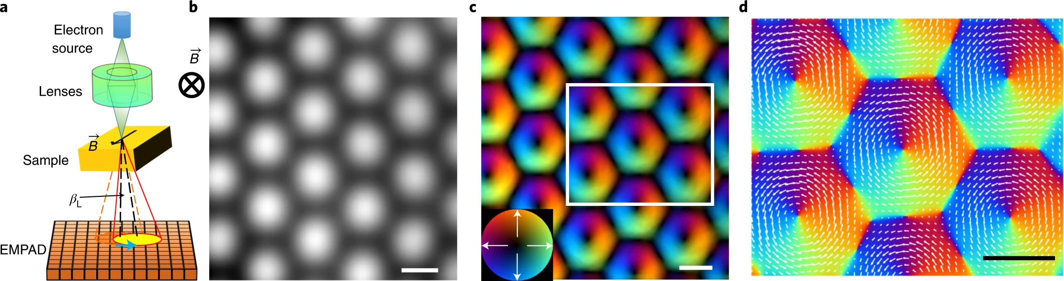
Lorentz Electron Ptychography (LEP)

  • Field-free objective lens (Lorentz mode): sample in remnant field → electrons deflected by Lorentz force
  • Aharonov–Bohm magnetic phase encoded in 4D-STEM diffraction patterns on a pixelated detector (EMPAD)
  • LEP reconstructs the magnetic induction map from overlapping probes (Chen et al. 2022)
  • Resolution set by maximum scattering angle with meaningful dose — not the probe-forming aperture (2–6× gain)
  • Corrects probe damping/distortion that limits CoM/DPC field measurements

Adapted from Chen et al. (2022) Fig. 1: Lorentz-mode 4D-STEM setup; SSB ptychographic reconstruction of a FeGe skyrmion lattice with in-plane field direction and vector map.

Note

Same ptychographic inverse problem as electrostatic imaging — the forward model now includes the magnetic Aharonov–Bohm phase

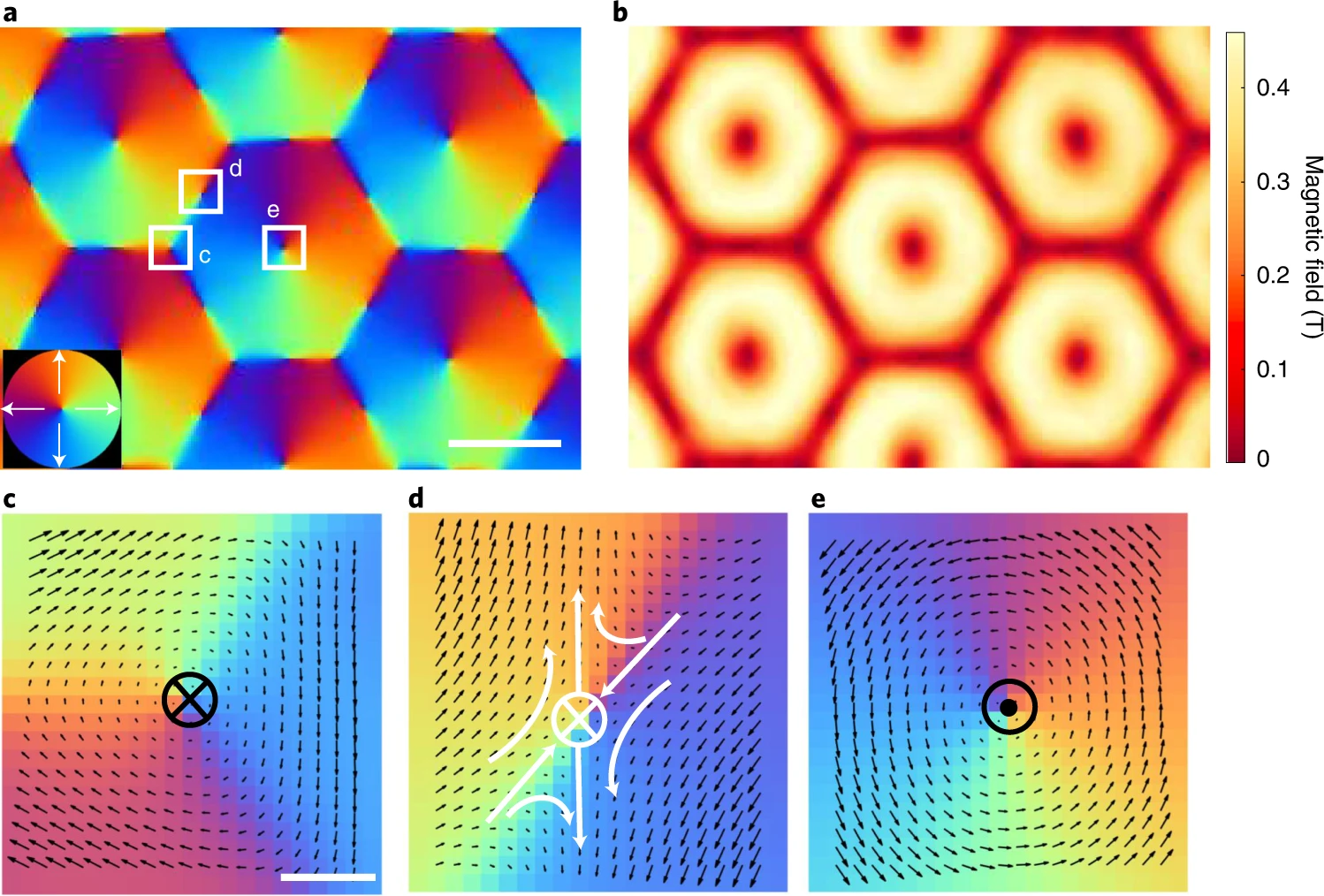
Skyrmion Internal Structure in FeGe (Fig. 2)

  • Model system: Bloch-type skyrmion lattice in FeGe single crystal (94 K, external field)
  • LEP maps lateral \(\vec{B}_\parallel\) direction and magnitude simultaneously (Chen et al. 2022)
  • Resolves internal spin textures invisible to LTEM, holography, or DPC:
    • counterclockwise vortex approaching skyrmion core
    • reversed (clockwise) vortex at triple junction
    • anti-vortex texture at skyrmion boundaries
  • Field direction well defined to ~1.2 nm from singular points (\(<20\) mT lateral field)

Adapted from Chen et al. (2022) Fig. 2: lateral magnetic induction direction (a) and magnitude (b) of a skyrmion lattice; zoomed vector maps at a corner (c), boundary (d), and core (e).

Note

High SNR near magnetization discontinuities — the regime where direct CoM methods fail

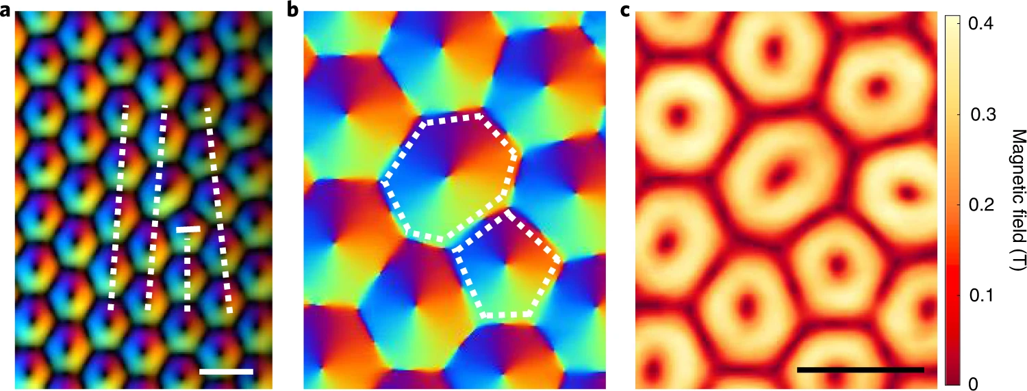
LEP: Topological Defects & Quantitative Advantage

  • Skyrmion-lattice edge dislocation: pentagon–heptagon pair at the core; distorted but topologically protected winding (Chen et al. 2022)
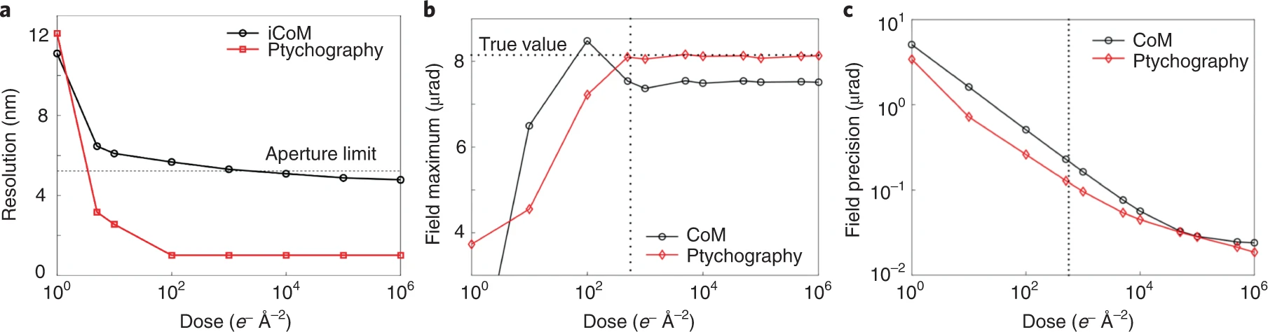
  • vs. iCoM/DPC at equal dose (Chen et al. 2022):
    • Resolution: LEP breaks the aperture limit (~5.2 nm probe) → ~1 nm at \(\gtrsim 10^2\) e⁻ Å⁻²
    • Accuracy: CoM underestimates field max by \(>10\)% (probe convolution); LEP matches truth at \(\gtrsim 500\) e⁻ Å⁻²
    • Precision: LEP superior at all doses; sub-10 nm features visible already at 1–10 e⁻ Å⁻²

Adapted from Chen et al. (2022) Fig. 3: skyrmion-lattice edge dislocation — magnetization direction near a 5–7 pair (top) and field magnitude at the core (bottom).

Adapted from Chen et al. (2022) Fig. 4: resolution, field maximum, and field precision vs. dose — LEP (red) vs. iCoM/CoM (black).

Note

Dose-efficient magnetic microscopy for magnetic materials

Outlook 1: From Imaging Static Structure to Imaging Dynamics

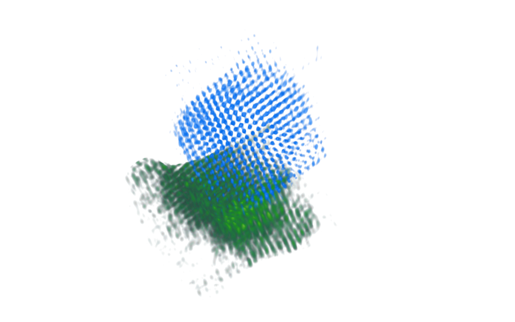
Open topics: - algorithms fast enough for real-time imaging –> in-situ ptychography - can we develop 3D depth sectioning methods fast enough for in-situ studies?

Note

We will see in-situ applications of ptychography as the codes become faster and more standardized

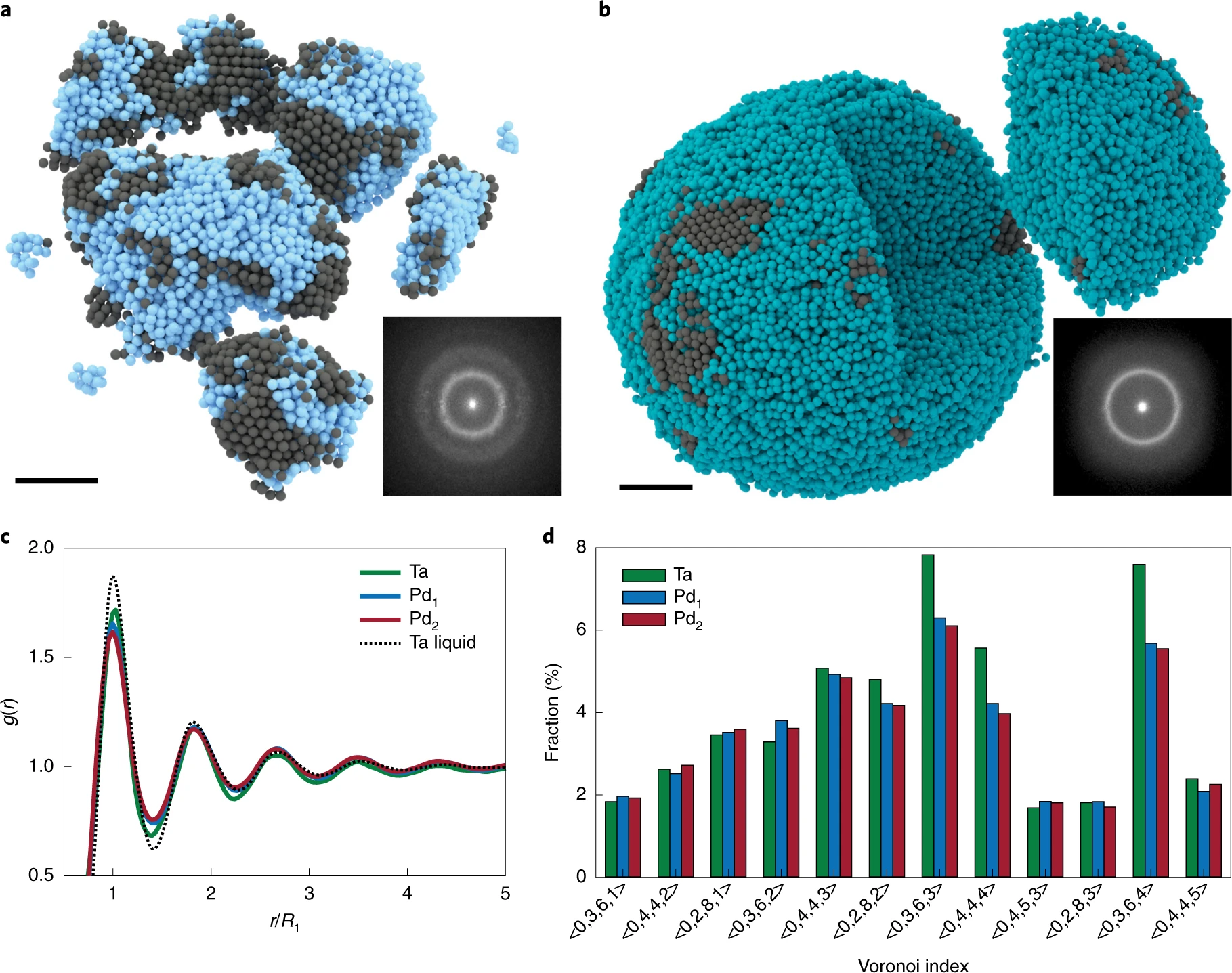
Outlook 2: From Imaging Ordered Structures to Imaging Disorder

  • Can we image weakly scattering amorphous materials in 3D? (Yuan et al. 2022)
  • Can we image the 3D structure of polymers?

Note

3D atomic packing in amorphous solids with liquid-like structure is already measurable by atomic electron tomography (Yuan et al. 2022)

Adapted from Yuan et al. (2022): 3D atomic packing in an amorphous solid with liquid-like structure.

Summary

  • Electron ptychography has a multitude of experimental settings to control and algorithms to explore
  • When tuned well, results well beyond hardware capabilities can be expected
  • Modern ML tools alleviate algorithm development and application by non-experts

Open positions at FAU

  • open Ph.D. / postdoc position in the ERC project HyperScaleEM, come talk to me if interested

References 📚

Ballabriga, Rafael, Jerome Alozy, Gabriel Blaj, et al. 2013. “The Medipix3RX: A High Resolution, Zero Dead-Time Pixel Detector Readout Chip Allowing Spectroscopic Imaging.” Journal of Instrumentation 8 (02): C02016. https://doi.org/10.1088/1748-0221/8/02/C02016.
Chen, Zhen, Yi Jiang, Yu-Tsun Shao, et al. 2020. “Mixed-State Electron Ptychography Enables Sub-Angstrom Resolution Imaging with Picometer Precision at Low Dose.” Nature Communications 11 (1): 2994. https://doi.org/10.1038/s41467-020-16688-6.
Chen, Zhen, Yi Jiang, Yu-Tsun Shao, et al. 2021. “Electron Ptychography Achieves Atomic-Resolution Limits Set by Lattice Vibrations.” Science 372 (6544): 826–31. https://doi.org/10/gkb46j.
Chen, Zhen, Yu-Tsun Shao, Steven E. Zeltmann, et al. 2024. Imaging Interstitial Atoms with Multislice Electron Ptychography. no. arXiv:2407.18063 (July). https://doi.org/10.48550/arXiv.2407.18063.
Chen, Zhen, Emrah Turgut, Yi Jiang, et al. 2022. “Lorentz Electron Ptychography for Imaging Magnetic Textures Beyond the Diffraction Limit.” Nature Nanotechnology 17 (11): 1165–70. https://doi.org/10.1038/s41565-022-01224-y.
Cipiccia, Silvia et al. 2024. “Fast X-Ray Ptychography: Towards Nanoscale Imaging of Large Volume of Brain.” The European Physical Journal Plus 139 (5): 434. https://doi.org/10.1140/epjp/s13360-024-05345-4.
Cui, Jizhe et al. 2024. “Imaging, Counting, and Positioning Single Interstitial Atoms in Solids.” arXiv Preprint arXiv:2407.18063.
Deimetry, M., T. C. Petersen, H. G. Brown, M. Weyland, and Scott D. Findlay. 2024. Differential Phase Contrast from Electrons That Cause Inner Shell Ionization. no. arXiv:2405.09043. https://doi.org/10.48550/arXiv.2405.09043.
Diederichs, Benedikt, Ziria Herdegen, Achim Strauch, Frank Filbir, and Knut Müller-Caspary. 2024. “Exact Inversion of Partially Coherent Dynamical Electron Scattering for Picometric Structure Retrieval.” Nature Communications 15 (11): 101. https://doi.org/10.1038/s41467-023-44268-x.
Ercius, Peter, Ian J. Johnson, Philipp Pelz, et al. 2024. “The 4D Camera: An 87 kHz Direct Electron Detector for Scanning/Transmission Electron Microscopy.” Microscopy and Microanalysis 30 (5): 903–12. https://doi.org/10.1093/mam/ozae086.
Frank, Joachim. 2022. “Chapter Three - Walter Hoppe — x-Ray Crystallographer and Visionary Pioneer in Electron Microscopy.” In Advances in Imaging and Electron Physics, edited by Peter W. Hawkes and Martin Hÿtch, vol. 221. The Beginnings of Electron Microscopy - Part 2. Elsevier. https://doi.org/10.1016/bs.aiep.2022.03.003.
Gilgenbach, Colin, Xi Chen, and James M LeBeau. 2024. “A Methodology for Robust Multislice Ptychography.” Microscopy and Microanalysis 30 (4): 703–11. https://doi.org/10.1093/mam/ozae055.
Gladyshev, Anton, Benedikt Haas, Thomas C. Pekin, et al. 2026. “Electron Ptychography Reveals Correlated Lattice Vibrations at Atomic Resolution.” Nature Communications 17: 5173. https://doi.org/10.1038/s41467-026-74135-4.
Henderson, Richard. 1995. “The Potential and Limitations of Neutrons, Electrons and X-Rays for Atomic Resolution Microscopy of Unstained Biological Molecules.” Quarterly Reviews of Biophysics 28 (2): 171–93. https://doi.org/10.1017/S0033583500003317.
Herdegen, Ziria, Benedikt Diederichs, and Knut Müller-Caspary. 2024. “Thermal Vibrations in the Inversion of Dynamical Electron Scattering.” Physical Review B 110 (6): 064102. https://doi.org/10.1103/PhysRevB.110.064102.
Hofer, Christoph, Jacob Madsen, Toma Susi, and Timothy J. Pennycook. 2025. “Detecting Charge Transfer at Defects in 2D Materials with Electron Ptychography.” Journal of Microscopy, ahead of print. https://doi.org/10.1111/jmi.13404.
Hoppe, Walter. 1983. “Electron Diffraction with the Transmission Electron Microscope as a Phase-Determining Diffractometer—from Spatial Frequency Filtering to the Three-Dimensional Structure Analysis of Ribosomes.” Angewandte Chemie International Edition in English 22 (6): 456–85. https://doi.org/10.1002/anie.198304561.
Jannis, Daen, Christoph Hofer, Chuang Gao, et al. 2022. “Event Driven 4D STEM Acquisition with a Timepix3 Detector: Microsecond Dwell Time and Faster Scans for High Precision and Low Dose Applications.” Ultramicroscopy 233: 113423. https://doi.org/10.1016/j.ultramic.2021.113423.
Jiang, Yi, Zhen Chen, Yimo Han, et al. 2018. “Electron Ptychography of 2D Materials to Deep Sub-ångström Resolution.” Nature 559 (7714): 343–49. https://doi.org/10.1038/s41586-018-0298-5.
Li, Guanxing, Ming Xu, Wen-Qi Tang, et al. 2025. “Atomically Resolved Imaging of Radiation-Sensitive Metal-Organic Frameworks via Electron Ptychography.” Nature Communications 16 (1): 914. https://doi.org/10.1038/s41467-025-56215-z.
Li, Pengcheng, Chenglin Pua, Zehao Dong, et al. 2025. Atomic-Scale Heterogeneity of Hydrogen in Metal Hydrides Revealed by Electron Ptychography. no. arXiv:2507.18906 (July). https://doi.org/10.48550/arXiv.2507.18906.
Li, Zhongbo, Harald Rose, Jacob Madsen, Johannes Biskupek, Toma Susi, and Ute Kaiser. 2022. “Computationally Efficient Handling of Partially Coherent Electron Sources in (s)TEM Image Simulations via Matrix Diagonalization.” Microscopy and Microanalysis, September, 1–9. https://doi.org/10.1017/S1431927622012387.
Llopart, Xavier et al. 2022. “Timepix4, a Large Area Pixel Detector Readout Chip Which Can Be Tiled on 4 Sides Providing Sub-200 Ps Timestamp Binning.” Journal of Instrumentation 17 (01): C01044. https://doi.org/10.1088/1748-0221/17/01/C01044.
Müller, Knut, Florian F. Krause, Armand Béché, et al. 2014. “Atomic Electric Fields Revealed by a Quantum Mechanical Approach to Electron Picodiffraction.” Nature Communications 5: 5653. https://doi.org/10.1038/ncomms6653.
Odstrçil, Michal, Maxime Lebugle, Tobias Lachat, Jörg Raabe, and Mirko Holler. 2019. “Fast Positioning for X-Ray Scanning Microscopy by a Combined Motion of Sample and Beam-Defining Optics.” Journal of Synchrotron Radiation 26: 504–9. https://doi.org/10.1107/S1600577519001309.
Ophus, Colin. 2019. “Four-Dimensional Scanning Transmission Electron Microscopy (4D-STEM): From Scanning Nanodiffraction to Ptychography and Beyond.” Microscopy and Microanalysis 25 (3): 563–82. https://doi.org/10.1017/S1431927619000497.
Pelz, Philipp M., Sinéad M. Griffin, Scott Stonemeyer, et al. 2023. “Solving Complex Nanostructures with Ptychographic Atomic Electron Tomography.” Nature Communications 14 (11): 7906. https://doi.org/10.1038/s41467-023-43634-z.
Pennycook, Timothy J., Andrew R. Lupini, Hao Yang, Matthew F. Murfitt, Lewys Jones, and Peter D. Nellist. 2015. “Efficient Phase Contrast Imaging in STEM Using a Pixelated Detector. Part 1: Experimental Demonstration at Atomic Resolution.” Ultramicroscopy, Special issue: 80th birthday of harald rose; PICO 2015 – third conference on frontiers of aberration corrected electron microscopy, vol. 151 (April): 160–67. https://doi.org/10.1016/j.ultramic.2014.09.013.
Poikela, Tuomas et al. 2014. “Timepix3: A 65K Channel Hybrid Pixel Readout Chip with Simultaneous ToA/ToT and Sparse Readout.” Journal of Instrumentation 9 (05): C05013. https://doi.org/10.1088/1748-0221/9/05/C05013.
Romanov, Andrey, Min Gee Cho, Mary Cooper Scott, and Philipp Pelz. 2024. “Multi-Slice Electron Ptychographic Tomography for Three-Dimensional Phase-Contrast Microscopy Beyond the Depth of Focus Limits.” Journal of Physics: Materials 8 (1): 015005. https://doi.org/10.1088/2515-7639/ad9ad2.
Sha, Haozhi, Jizhe Cui, and Rong Yu. 2022. “Deep Sub-Angstrom Resolution Imaging by Electron Ptychography with Misorientation Correction.” Science Advances 8 (19): eabn2275. https://doi.org/10.1126/sciadv.abn2275.
Skoupy, Radim, Elisabeth Müller, Timothy J. Pennycook, Manuel Guizar-Sicairos, Emiliana Fabbri, and Emiliya Poghosyan. 2025. “Ptychoscopy: A User Friendly Experimental Design Tool for Ptychography.” Scientific Reports 15 (1): 24959. https://doi.org/10.1038/s41598-025-09871-6.
Tate, Mark W., Prafull Purohit, Darol Chamberlain, et al. 2016. “High Dynamic Range Pixel Array Detector for Scanning Transmission Electron Microscopy.” Microscopy and Microanalysis 22 (1): 237–49. https://doi.org/10.1017/S1431927615015664.
Thibault, Pierre, and Andreas Menzel. 2013. “Reconstructing State Mixtures from Diffraction Measurements.” Nature 494 (7435): 68–71. https://doi.org/10.1038/nature11806.
Varnavides, Georgios, Willem P. M. de Kleijne, and Stephanie M. Ribet. 2026. “The ABCs of Phase Retrieval: Connecting the Acronyms of Scanning Transmission Electron Microscopy.” MRS Bulletin 51 (7). https://doi.org/10.1557/s43577-026-01100-3.
Visualization of Oxygen Vacancies and Self-Doped Ligand Holes in La\(_3\)Ni\(_2\)O\(_{7-\delta}\). n.d.
Yang, Hao, Peter Ercius, Peter D. Nellist, and Colin Ophus. 2016. “Enhanced Phase Contrast Transfer Using Ptychography Combined with a Pre-Specimen Phase Plate in a Scanning Transmission Electron Microscope.” Ultramicroscopy 171 (December): 117–25. https://doi.org/10/f9fwhk.
Yang, Wenfeng, Haozhi Sha, Jizhe Cui, Liangze Mao, and Rong Yu. 2024. “Local-Orbital Ptychography for Ultrahigh-Resolution Imaging.” Nature Nanotechnology, January, 1–6. https://doi.org/10.1038/s41565-023-01595-w.
You, Shengbo, Andrey Romanov, and Philipp M Pelz. 2024. “Near-Isotropic Sub-Ångstrom 3d Resolution Phase Contrast Imaging Achieved by End-to-End Ptychographic Electron Tomography.” Physica Scripta 100 (1): 015404. https://doi.org/10.1088/1402-4896/ad9a1a.
Yu, Yuchang, Kenneth A. Spoth, Marco Colletta, et al. 2025. “Dose-Efficient Cryo-Electron Microscopy for Thick Samples Using Tilt-Corrected Scanning Transmission Electron Microscopy.” Nature Methods 22: 2138–48. https://doi.org/10.1038/s41592-025-02834-9.
Yuan, Yakun, Dennis S. Kim, Jihan Zhou, et al. 2022. “Three-Dimensional Atomic Packing in Amorphous Solids with Liquid-Like Structure.” Nature Materials 21: 95–102. https://doi.org/10.1038/s41563-021-01114-z.
Zhang, Hui, Guanxing Li, Jiaxing Zhang, et al. 2023. “Three-Dimensional Inhomogeneity of Zeolite Structure and Composition Revealed by Electron Ptychography.” Science 380 (6645): 633–38. https://doi.org/10.1126/science.adg3183.